
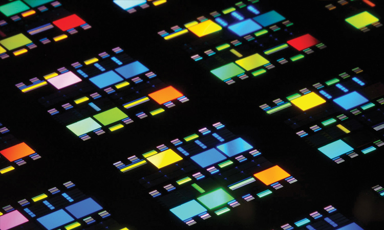
Silicon photonic crystals used to make memory devices, scattering light at various wavelengths. [Masaya Notomi]
Moore’s Law—the celebrated empirical prediction, put forward by Intel co-founder Gordon Moore a half-century ago, that the number of transistors on a single chip would double about every two years—is starting to approach some hard physical limits. Transistor gates are a mere 10 nanometers long today, and within a decade could measure just ten times the radius of a single atom.
In the end, however, such fundamental limits could prove irrelevant, as processors’ transistors don’t operate in isolation. They need memory to store data and instructions, as well as wires to connect them to that memory. Because the transistors dissipate energy when charging and discharging the wires, the energy consumed and heat emitted by an integrated circuit rises rapidly as the density and bit rate of components increases.
Researchers hope to use light not only to connect one computer to another but also to speed up computers’ internal operations.
According to Masaya Notomi, a physicist at the Basic Research Laboratories of Japanese telecommunications company NTT, this interconnection problem is likely to prove the real stumbling block for silicon chips. “Already half of a chip’s energy consumption is due to communications within it,” he says. “But as the communication bandwidth goes up, the energy needed to communicate a single bit will rise. This will lead to a bottleneck in 10 to 15 years from now.” (For more on interconnects, see “Optical Interconnects and Extreme Computing.”)
The answer, according to Notomi and a number of other researchers, could lie in photonics. The ability of light to carry information in different wavelength channels has already been exploited with dazzling success in the world’s fiber optic telecommunication networks. Now, researchers hope to use light not only to connect one computer to another but also to speed up computers’ internal operations—including new approaches to the memory and storage functions central to computing.
What about photonic processors?
Some envision an even broader future for photonics in computing—in which photonic memory schemes such as those discussed in this feature would ultimately complement photonic processors inside all-photonic chips. In fact, primitive photonic processors do exist.
Vladan Vuletić of the Massachusetts Institute of Technology (MIT) and colleagues have built the optical equivalent of a transistor by suspending a gas of supercooled cesium atoms between two mirrors. Usually those atoms allow beams of light—consisting of about 400 photons—to pass through. But if a single “gate photon” is fired into them from a different angle, bumping one of the atoms into a higher energy state, the atoms become opaque to light. In other words, a very weak beam of light switches a more powerful one on and off.
In another approach to a photonic switch, Minghao Qi of Purdue University in West Lafayette, Indiana and colleagues have built a device consisting of two waveguides separated by a small ring, all of which are etched onto a silicon chip. When a weak light pulse is sent along one of the waveguides it causes the ring to heat up and change its refractive index, which blocks a more intense beam of light in the other waveguide.
Such devices, while interesting, seem unlikely to challenge electronic processors anytime soon. The MIT setup, according to Vuletić, is a proof of principle rather than a practical template, although he speculates that the tiny artificial atoms known as quantum dots might one day yield a solid-state version. The Purdue device, while built in silicon, is thousands of times slower than electronic devices, and uses around a billion times more power. Qi hopes it will have more specialist applications, such as military aviation technologies that can withstand electromagnetic interference.
Some researchers, though, are highly skeptical about the potential for photonic processors, whatever the time frame. Rodney Tucker of the University of Melbourne argues that photonic logic circuitry does not have “even the remotest prospects” of providing commercial digital processing. One of the biggest challenges, he says, lies in logic-level restoration—the ability to maintain signals’ intensities at the standardized levels representing 0’s and 1’s as they propagate through a circuit. “This can be achieved naturally using CMOS transistors,” he maintains, “but it is nigh-on impossible in photonics.”
Beyond the straight and narrow
The concept of optical computing is nearly as old as the laser, and rests on the discovery of nonlinear optics that followed shortly after the laser’s invention in 1960. Digital computing itself relies on nonlinearity—that is, on a small change in a device’s input causing a much bigger change in its output. This phenomenon allows transistors to act as switches, the building blocks of logic gates and hence computers. Photons, unlike electrons, do not interact directly with one another, but the hope has been that laser-generated nonlinear interactions between light and matter might provide an intermediary that would allow optical computing.
Thus far, that approach has yet to really bear fruit. Over decades of research, scientists and engineers trying to build optical computers have encountered many technical problems, not least how to pump enough energy into tiny chips to create nonlinear effects without destroying the chips in the process. As much as five orders of magnitude more energy is needed to generate useful nonlinear processes in any known optical material than is needed to power a silicon transistor. A full-blown optical computer thus still looks like a distant prospect.
Yet photonics is beginning to make its mark on chip technology. Several high-tech companies, including Intel and IBM, have built chips that integrate electronic and photonic components. These chips can communicate with one another directly using light at up to 100 gigabits per second (Gb/s), rather than relying on external transceivers. That could in principle help tame the vast appetite for energy in data centers in particular, which currently consume about 2 percent of the U.S. electricity supply.
A more advanced lab version of an integrated-photonic chip was reported by Vladimir Stojanovic of the University of California in Berkeley and colleagues in December 2015. The Berkeley device contained 850 optical components—far more than the several dozen present on a chip unveiled by IBM seven months earlier—and reportedly could be built using fabrication methods consistent with a standard CMOS foundry.
Even this chip, however, still uses light as a mere data carrier. According to Wolfram Pernice, an electrical engineer at the University of Münster, Germany, simply speeding up data transmission between processor and memory will not be enough to relieve chips’ impending bottleneck. That’s because, he says, the need to convert optical into electrical data and vice versa at each end of the connection is itself inefficient.
And that’s where new research by a number of groups, including his own, comes into play—the effort to at least partly overcome the electro-optical conversion problem by replacing electronic memory with a purely photonic version.
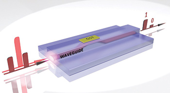 Read and write: The device made by Pernice’s group uses a germanium-antimony-tellurium (GST) ring that changes from a crystalline to an amorphous state (or vice versa) when struck by intense laser pulses , allowing storage of binary data. Illumination by weaker pulses then allows those data to be read out. [Carlos Rios / Oxford University]
A change of phase
Pernice and Oxford University electrical engineer Harish Bhaskaran lead an Anglo-German group that has made what the researchers describe as the first permanent (that is, non-volatile) purely photonic memory chip. They did so using the material GST, a compound of germanium (Ge), antimony (Sb) and tellurium (Te) used in rewriteable CDs and DVDs. The fact that GST can exist in two stable states—crystalline, like a metal, or amorphous, like glass—makes it well suited to storing binary data.
Using standard lithographic techniques, the researchers carved out a silicon nitride waveguide on a silicon oxide wafer, and then deposited a thin layer of GST to form a narrow ring around the waveguide. By sending an intense laser pulse through the waveguide they were able to melt the GST and change its structure from crystalline to amorphous; using a slightly less intense pulse they could then recrystallize it. In this way they could write binary data to the device, with one of the two states corresponding to a 1 and the other to a 0. A much weaker pulse of light sent through the GST ring allows the data to be read, as the pulse is transmitted far more readily when the ring is in the amorphous state.
As with CDs and DVDs, and unlike in previous photonic chips, this memory unit requires no power to retain its state. Indeed, says Pernice, it should hold data for years if not decades. In contrast to CDs and DVDs, however, it requires no external mechanical (spinning) device, which means its minimum bit size is not limited by the diffraction limit and that it is possible to read several bits at the same time.
Pernice and colleagues found that they could boost the device’s storage capacity by varying the intensity of the read and write pulses. They showed that by changing the fraction of the GST ring that was crystalline—in a range from completely crystalline at one extreme to entirely amorphous at the other—the ring memory could hold eight states (three bits) rather than just two states (one bit).
 Photonic-crystal memory: Notomi’s group has created a photonic-crystal lattice in which resonant cavities—the hole-free areas roughly four holes long in the SEM image above—provide a route to photonic memory. [Courtesy of Masaya Notomi]
This feature is shared by electronic phase-change memory, currently being developed by several semiconductor manufacturers. As Pernice points out, however, photonic memory can be switched more quickly—potentially in a few thousandths of a nanosecond, compared with the tens of nanoseconds typical of electronic phase-change memory. Photonic devices can also operate at several different wavelengths simultaneously, thereby enabling multiple read and write operations in different channels at the same time.
Bias needed
Notomi’s group at NTT in Japan has also produced an optical device that can store binary data by switching between two stable states. The device in this case is made from semiconductor photonic crystals, within which the scientists have created resonant cavities.
Under the scheme, a passing, “write” pulse of light tuned to a cavity’s resonant frequency can change the refractive index of the cavity, thereby writing data to the photonic memory. The change in the index value allows a second, “read” pulse of the same frequency to then pass through the cavity and register a 1 in a detector on the far side of the crystal. By contrast, if there is no initial write pulse and consequent change in refractive index, the second pulse is instead blocked, resulting in a 0.
The group’s device consists of multiple cavities, or bits, each with its own specific resonant frequency, which are placed in series and served by a single waveguide. This allows one beam of light containing a spread of frequencies to write data to specific bits. Using silicon, which is easy to etch, the researchers created 105 bits spaced at 8-μm intervals; using indium gallium arsenide phosphide and indium phosphide, which need less power to read and write data, they were able to manage 28 bits.
The device requires a faint but continuous bias beam to maintain bits in the 1 state; removal of the beam resets the bits to zero. Thus the unit cannot act as long-term storage, analogous to a hard drive. Instead, it would be used for certain kinds of random-access memory (RAM), which in current architectures is generally made up of capacitors and transistors. Being very small and very quick, says Notomi, the new memory would be used in high-performance computing and high-end network processors, rather than as general-purpose RAM.
Questions of power
In the drive to move photonic memory closer to practical use, power consumption could prove a stumbling block. Rodney Tucker, an electrical engineer at the University of Melbourne in Australia, points out that modern electronic RAM needs only about 3 femtojoules (fJ) to write a bit of data, whereas Pernice’s technology requires more than 13,000 fJ. Notomi says that his device can do this using just 1.6 fJ, but acknowledges that when the energy consumed by the bias pulses is taken into account, his group’s memory is likely to require more power than electronic memory. But where photonic memory has the edge, he says, is at high bandwidths. In those cases, he claims, slower electronic memory would require greater power levels altogether, because it would need to convert high-bit-rate data into low-bit-rate data and back again.
To show that their technology is ready to be commercialized, Notomi and colleagues plan to produce an indium-based device with 10,000 bits, each needing just a few nanowatts of power, within the next 10 to 15 years. The necessary compound-semiconductor fabrication, he says, “is increasing year on year.”
Pernice too acknowledges that commercialization won’t happen overnight. He and his colleagues have made three individual memory elements, whereas modern hard disks can contain billions of storage elements. Lab-based devices, he admits, contain too many defects to be built with anything like such densities, but he believes that industry could perfect the technology “within five or ten years.”
Into the quantum realm
The discussion so far provides a sample of research into photonic memory chips—as well as some idea regarding the community’s disagreement over their potential. Yet light-based memory is also being investigated as the basis of a very different kind of information processing—one that exploits the laws of the quantum, rather than the classical, world.
 Fiber stretch: The quantum memory devised by Laurat’s group involves a length of fiber suspended in a vacuum chamber and surrounded by a cloud of cesium atoms. The fiber is seen here as a faint line crossing the chamber. [Neil V. Corzo / Laboratoire Kastler Brossel]
As with work by Vladan Vuletić and colleagues at MIT (see sidebar above), research by a group at the Pierre and Marie Curie University in Paris involves interactions between light and a group of very cold atoms. Julien Laurat and co-workers stretched a piece of a commercial fiber optic cable so that it was just 400 nm in diameter, and surrounded the fiber with a cloud of about 2,000 cesium atoms chilled to within a fraction of a degree above absolute zero. They then carried out “electromagnetically induced transparency” by shining a laser on the atoms and changing the atoms’ properties so that they became transparent to another, weaker light pulse of just the right frequency.
What the researchers did was to reduce the intensity of the second pulse right down to the point where it was made up of less than a single photon on average. By turning off the first beam they were able to slow down and then halt the pulse so that it transferred its quantum state to the cesium cloud—the electromagnetic field from the pulse spilling outside the confines of the very narrow fiber. A few moments later, the researchers turned the first beam back on, and the single-photon pulse continued on its journey, with the collective excitation of the cesium atoms resulting in a collective, and therefore well-directed, emission back along the fiber.
Laurat and colleagues, in other words, showed that they could store the quantum information encoded in a single photon for a finite period. Single photons constitute the foundational data carriers in many quantum communication systems. Quantum key distribution, for example, allows the sender and receiver of a confidential message to share a key to encode and decode that message with complete security. But exchanging such keys over 100 km or more is tricky because, unlike classical data, quantum data in the form of light pulses cannot be boosted by amplifiers as they attenuate en-route. To do so would destroy the delicate quantum states involved.
Instead, devices known as quantum repeaters are needed. These would link two pairs of entangled particles in order to double the entanglement distance, with the linked pairs then in turn being linked to other linked pairs, and so on. However, because the linking process is probabilistic and often needs to be repeated several times to succeed, quantum repeaters must be able to store the quantum states of the two entangled particles that they link together—hence the need for quantum memory.
 Intense core: Cross-section of the hollow-core photonic crystal used by Ian Walmsley’s group. Cesium atoms are placed in the core, where the light field is at its most intense and strong light-matter interactions are possible. [Amir Abdolvand, Max Planck Institute for the Science of Light, Erlangen, Germany]
Like the Paris group, Ian Walmsley and colleagues at Oxford University, U.K., are developing photonic memory for use in quantum repeaters. [Walmsley is the 2016 vice president of The Optical Society.] The Oxford team also uses cesium atoms, but places those atoms in the core of a hollowed-out photonic crystal, rather than around a normal optical fiber. This enhances the interaction between atoms and light, so that experiments can take place at room temperature, which, says Walmsley, would make such memory simpler and smaller. But while Laurat’s group can store a photon for a few microseconds, Walmsley’s has so far been limited to just a few tens of nanoseconds, albeit at a higher bandwidth. As Laurat points out, several milliseconds will be needed to connect photons over hundreds of kilometers.
Tomorrow’s Internet
Ultimately, this kind of photonic memory could be used in quantum computers, as it would allow single photons to be cached so that they could be used together to execute quantum algorithms. But, as with fully optical computing, many believe that full-blown quantum computers could still be decades away. So for the moment, Laurat, like Walmsley, is concentrating his efforts on quantum communication.
Already, quantum key distribution is used commercially by banks and other organizations to encrypt messages over a few tens of kilometers. But Laurat and other physicists would like to see that capability extended to much larger distances, potentially leading to a planet-wide network of quantum links—the so-called “quantum Internet.” Quantum memory could also be used to carry out quantum state engineering, which involves generating and manipulating states that can be used to study fundamental aspects of quantum physics and that might underpin quantum information technology.
Whether photonics can challenge electronics in classical digital processing remains an open question. Still, the ability to switch at lightning speeds and operate across multiple wavelengths makes photonic memory an enticing prospect. Where light may really come into its own, however, is in the quantum realm, allowing data to be communicated and manipulated in ways that are impossible with conventional electronics. Laurat, for one, is in no doubt about light’s still untapped potential. “Quantum photonics is coming,” he says, “and could change the face of information technology.”
Edwin Cartlidge is a freelance science journalist based in Rome.
References and Resources
-
E. Kuramochi et al. Nat. Photon. 8, 474 (2014).
-
M.R. Sprague et al. Nat. Photon. 8, 287 (2014).
-
B. Gouraud et al. Phys. Rev. Lett. 114, 180503 (2015).
-
C. Ríos et al. Nat. Photon. 9, 725 (2015).
-
C. Sun et al. Nature 528, 534 (2015).
