
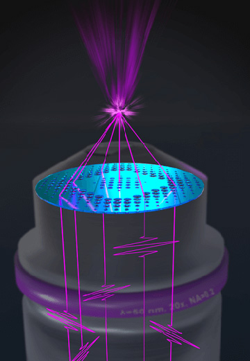
An artist’s view of a thin metalens that can focus extreme-ultraviolet (EUV) light through an array of nanoscale holes. [Image: Paulson School of Engineering and Applied Sciences, Harvard University]
Extreme-ultraviolet (EUV) light is very useful stuff, enabling the nanometer-scale lithography behind today’s most advanced semiconductor chips and forming the basis of ultrafast spectroscopy and attosecond science. But it’s very difficult light to work with.
In particular, EUV radiation’s ultra-short wavelengths—on the order of 50 nm or less—mean that this highly energetic light is absorbed by pretty much all materials. As a result, transmissive and refractive optics such as EUV lenses have been off the table. Instead, EUV radiation is controlled and concentrated by bouncing it off of specialized, bulky focusing mirrors in vacuum.
Now, researchers at Harvard University, USA, and the Graz University of Technology (TU Graz), Austria, have fabricated a new flat lens, or metalens, that reportedly can focus beams of EUV light to near the diffraction limit (Science, doi: 10.1126/science.adg6881). The team says that this novel optical element—created by turning conventional metalens-fabrication techniques on their head—lays the foundation for a “general-purpose transmissive optics technology for EUV radiation.”
That technology, the scientists believe, could enable the fashioning of ultra-high-resolution EUV microscopes for tracking charge carriers in semiconductors and solar cells at attosecond timescales. It could even, they suggest, allow for “a new generation” of EUV lithography meta-optics.
A hole new approach to meta-optics
Metasurfaces and metalenses are highly engineered surfaces that are decorated with forests of subwavelength-spaced nanostructures, the shape, size and spacing of which are tuned to diffract and channel light in specific ways. Given their potential to replace thick, bulky optics with highly compact, flat surfaces, research has exploded in the past decade on metasurfaces for controlling light at wavelengths ranging from the infrared to the visible. Meta-optics technology has even begun to make its way into commercial devices.
For EUV wavelengths, though, it’s been a different story. The usual route to creating a metalens or metasurface—dotting a surface with arrays of nanopillars or nanoscale bumps of dielectric material—won’t work for EUV light, since the light would be absorbed rather than refracted and controlled by those structures.
Marcus Ossiander, a postdoctoral associate at the Harvard lab of Federico Capasso, realized that one could potentially solve that quandary by taking a very different approach to building a metasurface. Instead of using arrays of positive features such as nanopillars, the metasurface could consist of arrays of nanoscale holes within a low-refractive-index material.
Instead of using arrays of positive features such as nanopillars, the metasurface could consist of arrays of nanoscale holes within a low-refractive-index material.
In this construct, the higher-index void area would act as a waveguide for EUV light, with the lower-index surrounding area acting like cladding on an optical fiber. Selecting metasurface materials with specific, low refractive indices would enable corresponding, specific EUV wavelength bands to be handled. And the metasurface’s transmission-phase and focusing characteristics could be tuned by varying the dimensions of the nanoholes themselves.
Tour de force of nanofabrication
To test out the idea, the Harvard team started out by selecting crystalline silicon as the host material for a prototype EUV metalens. The researchers then numerically compiled a “hole library,” mapping hole diameters to the corresponding predicted changes in transmission phase, to serve as a design resource. Using that library, they forward-designed a hole-dotted silicon metalens with a focal length of 10 mm that in principle could focus a beam of 50-nm EUV light to a tiny spot.
Next, in a nanofabrication tour de force, the team used a combination of chemical vapor deposition, reactive-ion etching, electron-beam lithography and other techniques to create arrays of holes with diameters ranging from 20 to 80 nm, as called for in the design. The result was a 1-mm-diameter, 200-nm-thin film containing hundreds of millions of holes. The work “pushed the limits of what’s possible in nanotechnology today,” Capasso said in a press release accompanying the research. “It was really a very large leap.”
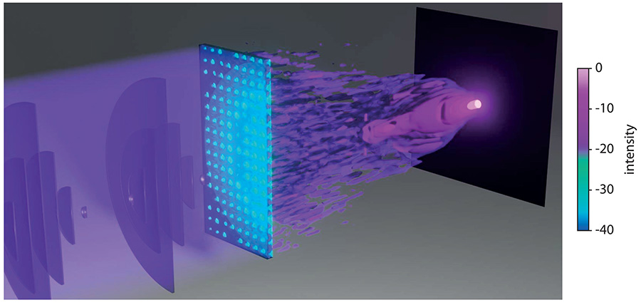
In a test of the prototype, the team sent attosecond EUV light pulses created by high-harmonic generation through the holey metalens, which variably altered the light’s transmission-phase characteristics to focus the beam to a tiny spot across a 10-mm focal length. [Image: Reprinted with permission from M. Ossiander et al., Science 380, 59 (2023)] [Enlarge image]
With the metasurface fabricated, the center of activity shifted from Harvard to Martin Schultze’s lab at TU Graz, where the metasurface would be tested using state-of-the-art attosecond EUV technology. There, the team fired 161-fs pulses of near-infrared, 1030-nm laser light into a jet of argon gas to create an attosecond EUV pulse train via high-harmonic generation (HHG), and sent that EUV beam through the holey metasurface. The resulting, tightly focused spot of EUV light—captured by a specialized CCD camera—indicated that the metalens was indeed working as advertised.
Toward an attosecond microscope
With the proof-of-concept in the bag, Ossiander, the Harvard postdoc who conceived the work, has now moved to TU Graz to work on applications, under a European Research Council (ERC) starting grant and other funding. Ossiander is particularly eyeing a metalens-based EUV microscope that could be used to track attosecond-timescale electronic processes in systems such as photovoltaic cells and semiconductors.
Beyond attosecond physics, the paper reporting the work also drops tantalizing hints about potential applications in EUV lithography. The paper’s authors appear to envision a sort of virtuous circle, with EUV lithography itself enabling the creation of ever more fine-grained, sophisticated metasurfaces—and with metasurfaces that can control EUV light, in turn, enabling “a new generation of lithography optics.”
The team stresses that the techniques and models it’s developed should, in principle, be transferrable directly to wavelengths shorter than the 50-nm EUV light that was focused by the proof-of-concept lens. Extending the system down to metalenses that can focus the 13.5-nm wavelengths important in EUV lithography, though, will represent something of a challenge. Such a metalens will need to be made of materials such as palladium, rhenium or ruthenium rather than silicon. And fashioning metasurface features at those tiny wavelengths, while feasible, pushes the limits of existing electron-beam lithography.