
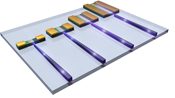
The research employed lateral aspect ratio trapping to grow a number of III–V photodetectors on a silicon-on-insulator substrate and couple the detectors to tapered silicon waveguides. [Image: The Hong Kong University of Science and Technology]
Scientists in Hong Kong and China have used a novel integration technique to efficiently couple compound-semiconductor photodetectors and silicon waveguides on industry-standard wafers (Optica, doi: 10.1364/OPTICA.468129). The researchers found that the new detectors could operate at very high data transfer rates and with low dark currents, arguing that these devices could, in the future, be complemented by integrated laser sources and thereby enable cheap, high-performance photonic integrated circuits on silicon.
Options for materials
By allowing fast, efficient communication at low costs, chip-based optical devices could potentially be exploited in everything from data-center interconnects to self-driving cars. The technology of choice for many is silicon photonics, given its compatibility with existing complementary metal oxide semiconductor manufacturing techniques. However, while researchers have already used silicon to make high-performance waveguides and modulators, they have yet to enjoy similar success when it comes to light sources and detectors.
The answer is to integrate other, better-suited materials—such as germanium or III–V compound semiconductors—into the silicon substrate. However, each integration technique has its downsides. Lasers and photodetectors made from III–V materials have shown excellent performance when bonded to silicon, but such bonding is expensive and hard to scale up.
Epitaxy, in contrast, involves building up integrated circuits by setting down one crystalline layer at a time—so enabling a single, monolithic structure made from multiple semiconductors to emerge. This approach has been used to grow III–V quantum-dot lasers and photodetectors directly on a silicon substrate, but requires buffer layers several micrometers thick between the compound semiconductors and silicon to limit defects. These, in turn, restrict the photonic coupling between the different layers.
Lateral aspect ratio trapping
The latest work explores how to overcome the buffer-layer problem by using what is known as lateral aspect ratio trapping. This involves adding atomic layers of different semiconductors along the horizontal direction of a patterned substrate, rather than stacking those layers on top of one another.
Kei May Lau of the Hong Kong University of Science and Technology and colleagues reported last year that they had used this technique to grow optically pumped lasers and high-performance III–V photodetectors directly on a platform combining silicon-on-insulator and indium phosphide. Now they have shown it is possible to couple the photodetectors to silicon waveguides.
The researchers made their integrated devices using a commercial 8-inch silicon-on-insulator wafer. They carved out silicon structures in a multi-step process comprising dry and wet etching, with those structures including both the waveguides and the lateral trenches within which the III–V semiconductor was then added to form the complete circuit.
The upshot was a number of tapered waveguides coupled to photodetectors of differing lengths via air gaps a few hundred nanometers long. Each detector comprised a p-i-n junction a few micrometers wide that was made up of an n-layer of indium phosphide, an absorbing i-region of indium phosphide and indium gallium arsenide, and a p-layer of indium gallium arsenide.
Results and future directions
Carrying out a range of tests on their integrated photodetectors, Lau and colleagues showed that they could comfortably outstrip previously demonstrated devices. They were able to pick up signals across the entire telecommunications band, and do so at rates of up to 112 gigabits per second. They found that the detectors had dark currents of just 60 picoAmps, and estimated their system’s coupling efficiency to be as high as 70%.
The researchers say that their system can be improved in a number of ways, such as tailoring the detectors’ metal contacts for radiofrequency performance and reducing the length of the gaps between photodetectors and waveguides while filling the gaps with oxides or other dielectric materials. Once optimized, however, the scheme ought to be very versatile. By appropriate patterning of the silicon-on-insulator wafer guiding the growth of the III–V semiconductors, they say it should be possible to fashion a range of devices within the same chip—including lasers.
The results from their waveguide-coupled photodetectors, they say, “prove their capability for practical applications in optical communications and provide a promising solution for fully integrated silicon photonics.”