
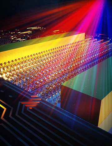
Artist’s impression of the thin, ultrafast photodetector. [Ella Marushchenko]
Over the past few decades, all kinds of electronic devices have become smaller, lighter, faster and vastly more capable. Why should photodetectors be any different?
To answer that question, researchers based in Melbourne, Australia, have devised a thin, lightweight photodetector made from a sandwich of printed nanometer-scale layers of tin monosulfide (Adv. Mater., doi:10.1002/adma.202004247). The chip-like device picks up wavelengths all the way from deep ultraviolet to near-infrared, and its responsivity to red light is up to three orders of magnitude higher than that of commercial photodetectors.
The next generation of imaging systems, light detectors and artificial systems will require significantly miniaturized photodetectors, says Sumeet Walia, associate professor of engineering at RMIT University in Melbourne. That need inspired the photodetector study, he adds.
Atomically thin is in
Following the discovery of graphene’s fascinating properties, scientists have been examining the optical and electronic properties of many other types of 2D crystals. One type of semiconductor, called the group IV monochalcogenides—compounds with one atom of tin, germanium or lead and one atom of sulfur or selenium—has interesting optoelectronic properties, but up until now, it has been difficult to fabricate large enough 2D sheets of the material for proper experimentation. Typical crystal-growth techniques such as vapor deposition cannot produce atomically thin layers of tin monosulfide without introducing defects and impurities.
Instead, the team tried a different manufacturing technique. The researchers heated tin inside a box filled with hydrogen sulfide gas. As the tin became molten, a sulfide layer formed on its surface. The team then lowered a silicon dioxide substrate onto the molten material, and the van der Waals forces between the tin monosulfide and the silicon dioxide made a single-unit-cell-thick layer of the tin compound adhere to the substrate. Next, the group built detectors from one, two and three layers of the ultrathin semiconductor and measured the amounts of current they generated under illumination.
The detectors picked up light of wavelengths all the way from 280 nm (the UV-B band) to 850 nm (near-infrared). The researchers noted that, unlike some other proposed thin-film photodetector materials such as cadmium and black phosphorus, tin monosulfide consists of widely available elements in a chemically stable compound, and the atomically thin layers formed in their experimental process are stable.
Chip integration
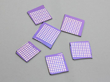
Close-up view of the photodetectors. [RMIT University]
Walia and his colleagues hope their work will find use in the next generation of optoelectronic devices. “The next step would be to develop imaging arrays and practical demonstrations of this device integrated with a transistor on a single CMOS chip,” he says. “This has been a huge technological bottleneck that we have aimed to overcome. Concurrently, the ability of the material to absorb a wide portion of the light spectrum makes it extremely exciting to create artificial-vision systems and applications such as photography in low-lighting conditions.”
The research group included scientists from the University of Melbourne, Australian National University, Monash University and University of New South Wales, all in Australia, as well as the Council of Scientific and Industrial Research, India.