
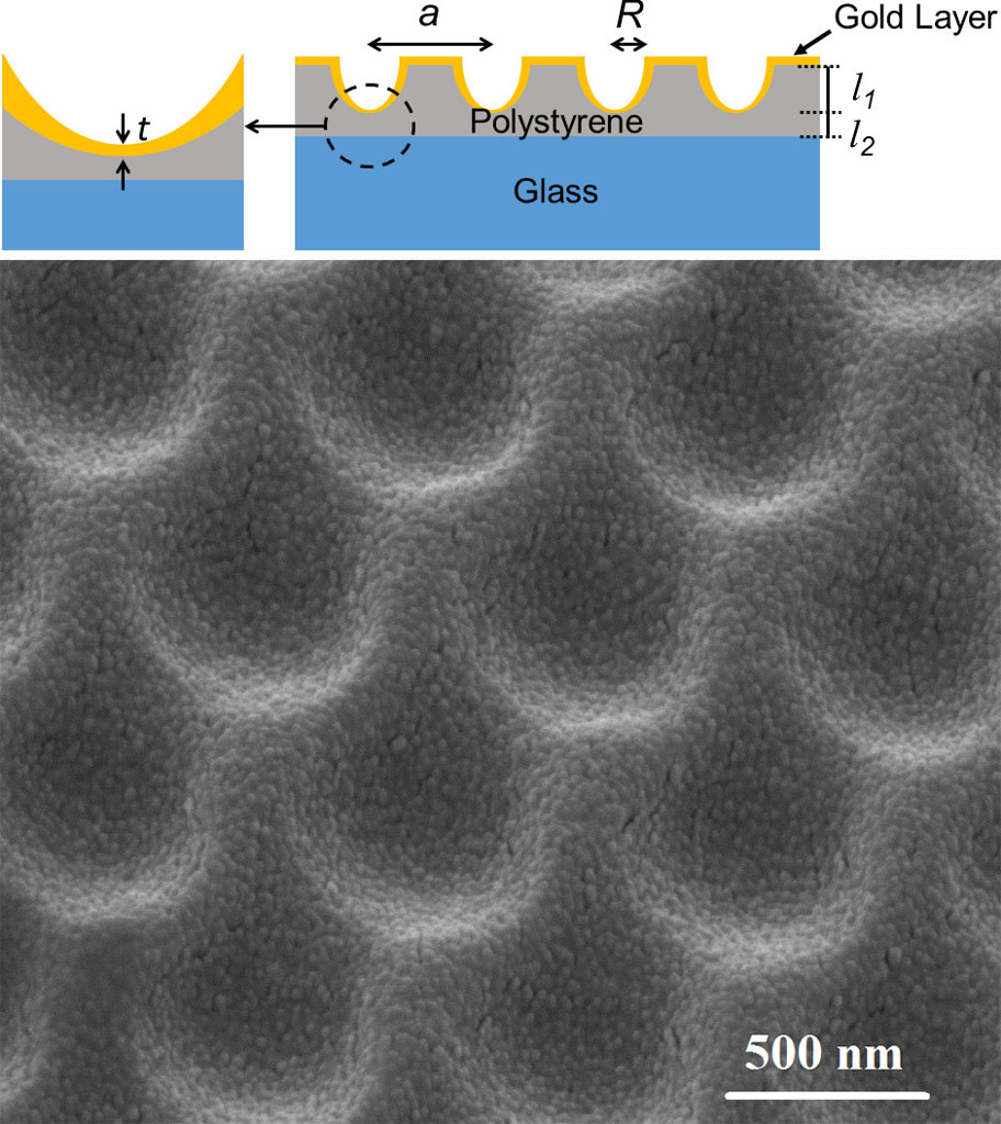
The researchers’ technique involves sputter-coating a substrate of nanocups pressed into a polystyrene base (bottom) with a thin gold layer (top). Optical enhancement comes from thickness variations in the gold film. [Images: Courtesy of Akshit Peer] [Enlarge image]
Researchers at the U.S. Department of Energy's Ames Laboratory and Iowa State University (ISU), USA, have reportedly demonstrated a technique for achieving extraordinary optical transmission, with modeled electric-field enhancements as high as a hundredfold, using a continuous film of gold on a corrugated, “nanocupped” substrate (Nanoscale, doi: 10.1039/c5nr07903a). The technique, according to the team, requires only soft-lithography fabrication, and can create comparatively large-area films. Those attributes, in the view of the scientists, compare favorably with the complex fabrication and tiny functional areas of conventional nanohole arrays—and could make the nanocup approach competitive for devices such as biosensors, solar cells and more.
The trouble with nanoholes
The ability to enhance light transmission using subwavelength-scale hole arrays in metal films, discovered nearly 20 years ago, has spurred considerable effort in plasmonics and other areas. But according to ISU professor Rana Biswas and grad student Akshit Peer, the authors of the new paper, nanohole arrays constitute a costly platform for experimenting with these effects, involving complex lithography and etching. Those techniques, further, commonly result in structures less than a millimeter square, which in turn necessitates a complex setup of an optical microscope tied to a spectrophotometer to measure experimental results.
Biswas and Peer scouted around for a less complex, more scalable method. They found it in a scheme that does not require the creation of holes, but only tiny periodic indentations a gold-covered substrate—with variations in the gold thickness, down to subwavelength scales, offering the key to optical enhancement. The result, they believe, is a “much simpler,” workbench-scale approach to creating these structures.
Soft lithography
To make their nanocup arrays, the team began with a pattered polycarbonate array of roughly 500-nm-diameter nanocups ordered from a commercial vendor. Using that as a master, they poured an elastomer, polydimethylsiloxane (PDMS), onto the cup array, and peeled off the material after curing. This left them with a positive PDMS mold of periodic “nanobumps” that could be used to stamp the pattern into another material.
Next, the researchers, spin-coated a glass slide with a thin layer of polystyrene, and pressed the PDMS stamp into the polystyrene at a high temperature for 45 minutes. Once the material had cooled, they removed the stamp, leaving behind a nanocupped polystyrene film on the glass slide. As a final step, the scientists sputter-coated the nanocupped substrate with gold film—positioning the slide at an angle in the sputter chamber, and rotating it, to obtain a varying thickness in the continuous film.
Optical results
The result, Peer and Biswas report, is a continuous metal film on a corrugated surface that shows extraordinary optical transmission of twice the classically expected value at wavelengths approaching the nanocup period. Because the method allowed the fashioning of relatively large-area structures of an inch square or more, they were able to measure these values using a conventional spectrophotometer, rather than a complex microspectrophotmeter setup. Numerical modeling by the team suggests that the optical enhancement they found stems from the thickness variations of the gold film—down to as thin as 25 to 30 nm, or less than the optical skin depth, at the nanocup bases.
According to Peer, an OSA student member, the ability both to inexpensively create these large-area films and to straightforwardly measure their optical properties makes them a potentially great platform for experiments and applications in plasmonics, sensing, photovoltaics and elsewhere. As one proof of concept in the biosensing arena, he and Biswas showed that depositing a 5-nm-thick dielectric film on the surface—mimicking the thickness and refractive index of a protein bilayer—resulted in a detectable redshift in the extraordinary-transmission peak.