
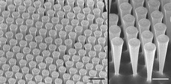
Scanning electron microscope image of “light funnels” etched in silicon substrate (scale bars: left, 5 microns; right, 1 micron). Funnels measure about 800 nanometers in diameter above and run down to about a hundred nanometers at the tip. [Image: S. Schmitt / MPL]
The cone cells—retinal photoreceptors that enable bright-light color vision in the human eye—are among the most familiar structures in biology. Scientists in Germany have now used a region of the retina that’s especially dense with cones, the fovea centralis, as inspiration for a new solar-cell configuration (Sci. Reports, doi: 10.1038/srep08570). According to the team’s modeling, these close arrays of “light funnels” can achieve substantially greater absorption and power conversion efficiencies than some other recently tested architectures.
The cone-packed fovea centralis is the area of the retina that’s responsible for high-acuity binocular vision in brightly lit situations. The efficiency of the cones in trapping incoming light in this part of the retina suggested to the research team, led by Silke Christiansen of the Max Planck Institute for the Science of Light, Germany, that a similar approach, implemented in silicon, could improve the efficiency of solar cells.
Previous studies had already suggested that arrays of vertical cylindrical silicon nanowires could operate well as light collectors. Building on that foundation, Christiansen’s team first used 3-D finite-difference modeling and optoelectronic simulations to gauge the effect on solar-cell efficiency of modifying these nanowire carpets into a light funnel geometry, consisting of an array of closely spaced inverted cones.
The team found that the light funnel arrays produced an absorption enhancement of some 65 percent relative to thin films, nearly double the enhancement experienced from an ordinary nanowire array. And the electrical simulations revealed that the arrays of cones could attain 60 percent higher power conversion efficiency than similarly sized nanowire arrays.
In addition to the modeling work, the team demonstrated, as a proof of concept, the fabrication of a light funnel array, using what the scientists maintain is “a low-cost technique” compatible with conventional semiconductor manufacturing processes. The technique begins with the deposition of polystyrene nanospheres atop a silicon wafer substrate, followed by reactive ion etching (with a controlled flux of reducing fluorine ions used to create the conical taper) to fashion the cones beneath the nanospheres.
In the wake of this work, Christiansen’s team will focus on implementing the light funnel design into robust, working thin-film solar cells and scaling the technology up into large-area photovoltaics. The team is also looking at other possible applications for the fovea-inspired design, such as LEDs and sensors. “The first pilot studies are so promising,” Christiansen says, “that we are confident these applications will not have to remain the stuff of dreams.”