
[Left panel] The MoS2 film was transferred from a sapphire substrate, at left, to a SiO2/Si substrate, at right. [Right panel] Detail of the transferred monolayer shows a lack of wrinkles, cracks, and other surface imperfections. [Image: Gurarslan et al., ACS Nano, doi: 10.1021/nn5057673]
Semiconducting films made from molybdenum disulfide (MoS2)—which are only a single atom thick—have gained much recent attention for their possible use in atomic-scale lasers, LEDs, photodetectors and other devices. But the material comes with a problem: How to move these delicate, ridiculously thin films from their growth substrates to the devices on which the films will actually be used. A team of engineers at North Carolina State University, USA, has now come up with one possible answer: Just add water.
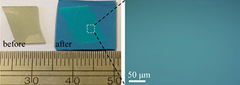
MoS2 is an example of a 2-D transition metal dichalcogenide (TMDC), a class of materials that is emerging as an alternative to a more familiar 2-D material, graphene, owing in part to their favorable band gap characteristics for some optical applications. But to work in practical, flexible devices, the TMDC must be transferred from the inflexible substrate used to grow the material to the flexible substrate used in the device—without cracks, wrinkles or other surface imperfections. And the transfer techniques that have been established for graphene don’t work well for MoS2.
To create a new technique for transferring MoS2 films, the North Carolina team took advantage of a specific characteristic of this material: its hydrophobic (water-repelling) properties (ACS Nano, doi: 10.1021/nn5057673). Specifically, they grew the atomically thin, hydrophobic semiconductor film atop a robust and hydrophilic (water-attracting) sapphire substrate.
The process of transferring the film from the sapphire substrate to a flexible one begins with simply applying a drop of water to the system, and nudging the material to allow the water to seep in, breaking the seal between the hydrophilic sapphire and the hydrophobic MoS2. The atomically thin film, now separated from the substrate and sitting atop the water droplet like a film of oil, can then be lifted—literally with tweezers—and placed on a flexible substrate for use in a photonic or other device. A video provided by the lab depicts the procedure.
The team believes that this surface-energy-driven method—demonstrated in this research for MoS2 films more than one centimeter wide and one atom thick—can be extended more generally to other 2-D materials. The group is now focused on applying the technique to actual devices. Meanwhile, according to the paper’s senior author, Linyou Cao, the work “gets us one step closer to using MoS2 to create flexible computers.”