
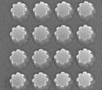
A scanning electron microscope image of a nanostructure array on freestanding aluminum films of nanogears. Credit: Purdue University
Researchers are looking to 3-D crystalline metallic nanostructures for advanced technologies in plasmonics, electronics and biosciences, because of these structures’ exceptional ability to control light. But these structures are difficult to make with existing fabrication techniques. Now, an international team of scientists has developed an easier, cost-effective method for creating the nanostructures using a bench-top system for laser shock imprinting (LSI) (Science, doi: 10.1126/science.1260139). With LSI, the researchers can fabricate smooth, large-area 3-D crystalline nanostructures at ambient conditions from thin sheets of metal.
Other methods for manufacturing 3-D crystalline metallic nanostructures involve electron beam lithography or template stripping, which can be time-consuming, expensive, inexact and work only for a few relatively soft metals. With LSI, the researchers were able to create 6-inch wafers of ultra-smooth 3-D crystalline nanostructures in about 30 seconds at room temperature from sheets of aluminum, copper, gold, silver and hard metals like titanium, as well as sheets of metal-graphene hybrids. LSI has the added benefit of mechanically strengthening the nanostructures.
The team, led by Gary Cheng at Purdue University (USA), demonstrated its method using a Nd:YAG laser pulse to irradiate a graphite ablation coating over a metal sheet. The laser pulse creates a shock wave that moves through the metal sheet, causing it to conform to an underlying silicon mold. During the stamping process, the metal maintains its crystalline structure and its electromagnetic and optical properties. (Normally, when metals recrystallize they form grains that roughen the structure and increase electrical resistance.) Cheng and his group created 3-D nanostructures with a variety of shapes, including pyramids, fishnets, bars, gears, v-grooves and trenches, with aspect ratios as high as five—an important value for plasmonic and sensing metamaterials.
The authors believe their LSI technique is versatile and scalable and could enable high-throughput fabrication of ultrasmooth 3-D nanostructures for high-speed electronics, advanced sensors and flexible solar cells. The metal-graphene hybrid structures could create metamaterial-based perfect absorbers for applications in optoelectronics and wireless communications.
There are, however, limitations to the LSI technique: the silicon molds are expensive to make (even though they can be reused hundreds of times), and it’s difficult to transfer the 3-D nanstructures onto different substrates.