
Feature
Optical Lithography in the Extreme UV
As the number of transistors on a chip continues to increase, the industry’s shrinking feature size is outstripping even the best efforts of optical engineers. Extreme ultraviolet lithography can lead to a more-than-tenfold decrease in wavelength, translating to a startling leap in performance.
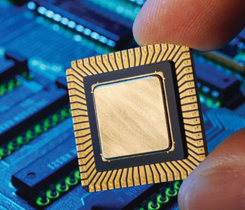
Semiconductor lithography is the art and science of printing integrated-circuit chips. The central processing unit in a desktop computer was printed using a wide array of capital equipment in a semiconductor fab belonging to a company like Intel or IBM. For leading-edge circuits, the linchpin of manufacturing equipment is a photolithographic wafer scanner, which projects a circuit-pattern image to a silicon wafer.
…Log in or become a member to view the full text of this article.
This article may be available for purchase via the search at Optica Publishing Group.
Optica Members get the full text of Optics & Photonics News, plus a variety of other member benefits.