
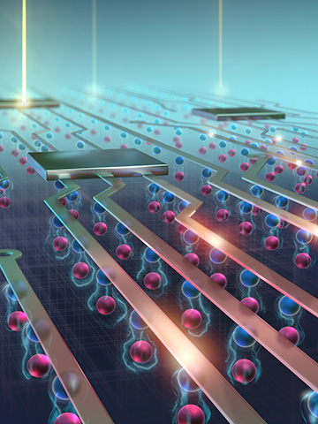
The researchers from EPFL in Switzerland and the National Institute for Materials Science in Japan envision circuits in which excitons—electron-hole pairs (red and blue balls)—act as carriers, controlled by laser light and by voltage biases applied at graphene electrodes (rectangular patches). [Image: LANES EPFL]
A nagging efficiency bottleneck in today’s communications networks is the need to convert between the optical signals that transmit data over long distances, and the electrical signals used in data processing. One potential solution lies in devices that manipulate not electrons or photons, but “excitons”—the bound electron-hole pairs formed when photons excite electrons in a semiconductor. But thus far, the “excitonic” devices demonstrated using bulk semiconductor materials have had to operate at frigid temperatures, a disadvantage that has held back practical applications.
Now, a Swiss-Japanese research team has used an ingenious stack of 2-D materials to develop a key component for practical excitonics: an excitonic transistor that can operate at room temperature (Nature, doi: 10.1038/s41586-018-0357-y). The prototype device could, the researchers believe, open the door to a generation of excitonic devices using 2-D materials. Those devices, in turn, could allow compact, energy-efficient optical-electronic interconnects, not only in communications but for a variety of other applications.
Electrons and holes
When a photon of the right frequency (and, thus, energy) is absorbed by a semiconducting material, it kicks an electron up to the semiconductor’s higher-energy conduction band—leaving behind a positively charged “hole” in the valence band. The electron and hole, still bound by Coulomb attraction, form a “quasiparticle” called an exciton. The exciton eventually disappears when the electron and hole recombine, releasing another photon.
In recent years, interest has burgeoned in “excitonic” systems that rely on the manipulation of these quasiparticles, analogous to the way that electronic systems rely on the manipulation of electrons. Such systems, it is thought, could offer an efficient way to convert between photonic and electronic systems in communications networks and other settings—since excitons are, in a sense, natural intermediates between photons and electrons.
Practical excitonics will require devices, such as excitonic transistors, that allow “currents” of excitons to be controlled. Researchers have had already some success in creating excitonic transistors in bulk semiconducting materials. But those devices have had to operate at temperatures below –173 °C, because of the low binding energy of excitons in these bulk materials.
One possible resolution to the quandary lies in 2-D materials, such as graphene and transition-metal dichalcogenides (TMDs). These materials have much higher exciton binding energies than bulk semiconductors, and thus could allow excitons to be created and manipulated at room temperature. But there’s a catch: excitons in these monoatomic layers don’t hang around for long, with lifetimes of only around 10 picoseconds. Moreover, excitons, as electron-hole pairs, are electrically neutral. Thus it’s hard to manipulate them using an in-plane electric field in a 2-D material.
The heterostructure difference
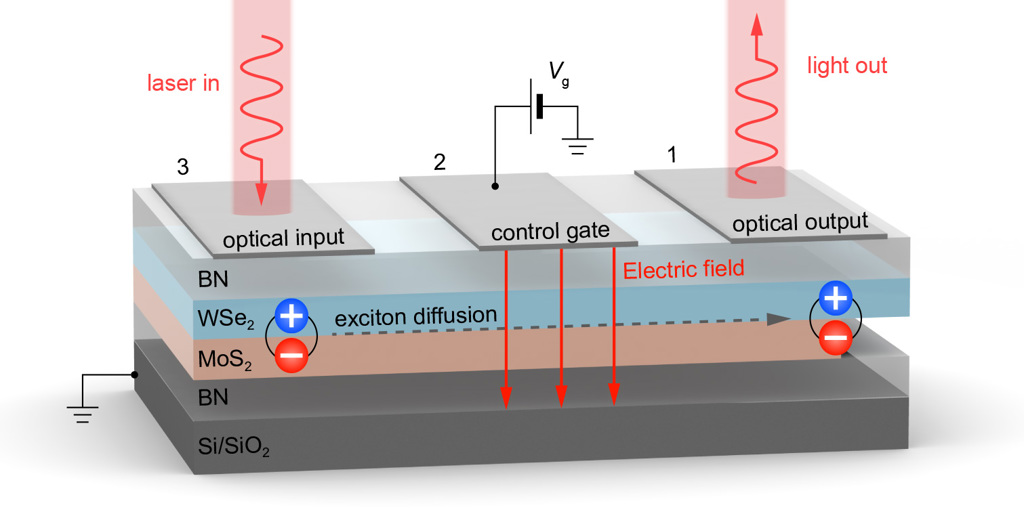
Schematic of the excitonic transistor developed by the Swiss-Japanese team. Fragments of transparent graphene (1, 2, and 3) act as gating electrodes that control the movement of excitons (electron-hole pairs) through a heterostructure consisting of tungsten diselenide and molybdenum disulfide. A hexagonal boron nitride shell encapsulates the device. [Image: LANES EPFL] [Enlarge image]
The Swiss-Japanese research team, led by Andras Kis of the École Polytechnique Fédérale de Lausanne (EPFL) and including other scientists from EPFL and Japan’s National Institute for Materials Science, found a solution to both problems. They did so by using not a single 2-D material, but a heterostructure made of several such materials.
At the heart of the system are layers of two atomically thin TMDs, molybdenum disulfide (MoS2) and tungsten diselenide (WSe2). Because of the differing band structure of the two materials, when an exciton is created in the heterostructure (for example, by absorption of a photon), the electron tends to reside in the MoS2 layer, while the hole stays in the WSe2 layer. The result is a system in which the exciton “lives” not in a single 2-D material layer, but between the two layers.
Such an interlayer exciton, it turns out, has a spatial separation between the electron and the hole that’s large enough to allow the exciton to survive 100 times longer than it would in a single 2-D material layer. Yet the exciton can still exist and thrive at room temperature. Further, the two-layer structure means that the exciton has a built-in out-of-plane dipole moment. That means it can be manipulated and controlled by an electric field and voltage bias in ways that would be impossible with excitons in a single 2-D layer.
Graphene gates
To build a working excitonic transistor, the team created the MoS2–WSe2 heterostructure, and encapsulated it in yet another material, hexagonal boron nitride (BN). On top of that BN shell, the researchers laid down multiple fragments of transparent, few-layer graphene to act as gating electrodes. The team then used a 647-nm laser diode to optically pump interlayer excitons on one end of the transistor structure, and used a CCD camera to measure emitted radiation from the structure.
The team found that the interlayer excitons were sufficiently long-lived to diffuse across a distance as long as five microns within the structure before recombining and emitting light. Further, the flux of excitons could be controlled and manipulated electrically by applying different voltage biases using the graphene electrodes, in transistor-like fashion.
Practical excitonics ahead?
The researchers argue that their results “make a strong case for integrating two-dimensional materials in future excitonic devices to enable operation at room temperature.” Such devices, they believe, could prove more energy efficient and compact than previously demonstrated fast optical switches, the comparatively large size of which (approximately 10 microns) limits their on-chip packing density. The team concludes that the prototypes it has demonstrated “could open the way for wider studies and applications of excitonic devices in the academic and industrial sectors.”