
Engineers have shown how 2D materials such as graphene can enable the growing of thinner and therefore smaller LEDs for vertical stacking, which could potentially prove a boon for advanced headsets and larger displays.
Augmented- and virtual-reality headsets require displays with exceptionally high resolution. But current technology based on light-emitting diodes (LEDs) struggles to make colored pixels small enough for the desired detail—sometimes causing users to see stripes between pixels.
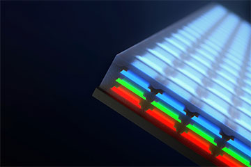
Now a US-led group of researchers claims to have shown how to potentially triple the density of LEDs in a display by stacking red, blue and green emitters on top of one another rather than laying them side by side, as is usually the case (Nature, doi: 10.1038/s41586-022-05612-1). They say they have demonstrated the highest ever density of micro-LEDs operating across the visible spectrum, and that their stacking technique could enable full-color displays for augmented and virtual reality as well as improving the resolution of televisions, smartphones and other larger-scale devices.
Stacking inorganic LEDs
Most digital displays today use LEDs made from organic semiconductors. These emitters are bright, light and relatively efficient, but they have shorter lifetimes than their inorganic equivalents and are reaching a lower limit on their size—thereby restricting display resolution.
To reach higher resolutions, researchers are trying to increase the packing density of inorganic micro-LEDs. These are made by separately growing very thin layers of crystal on wafers for each of the red, green and blue emitters, then extracting the crystals from their respective substrates and arranging them side by side to create individual pixels. However, misalignment can mean having to scrap entire devices, making it very difficult to achieve the sub-10-µm densities needed for augmented and virtual reality.
Vertical arrangements of LEDs could in principle triple the pixel density by having red, green and blue emitters share the same area on the screen. They have the additional advantage of avoiding individual placement—the three types of LED are laid on top of one another in the form of large-area membranes that are then divided up to create individual pixels.
However, this approach too has its problems. In particular, the conventional techniques used to extract indium gallium nitride−based LEDs from their substrates require those LEDs to be undergirded by a thick buffer layer to minimize dislocations and prevent laser-induced damage. As a result, each of the resulting LED films are around 5-10 µm thick, which in turn imposes a lower limit on their lateral dimensions because high-resolution lithography works best on relatively shallow chips.
2D transfer
The new research was carried out by Jeehwan Kim, Jiho Shin and colleagues at the Massachusetts Institute of Technology, USA, together with co-workers from other institutes in the US, the Republic of Korea and France. The researchers say they were able to overcome the problem of thick LEDs by using a technique they had previously developed known as 2D material−based layer transfer. This involves growing extremely thin layers of single-crystalline LEDs on two- rather than three-dimensional interlayers—materials that are mechanically flexible and help reduce interfacial strain.
Kim and colleagues used the technique to make the three different-colored LEDs—aluminium gallium arsenide on a graphene-coated gallium arsenide wafer in the case of the red emitters and indium gallium nitride on hexagonal boron nitride-coated sapphire wafers for the green and blue ones. With each LED measuring just 1-2 µm thick, they were able to make vertically integrated pixels with heights of around 9 µm. This total includes the pixel substrate and the layers between the different-colored LEDs, which serve both as glue and absorbers to limit light from the uppermost emitters interfering with the operation of those lower down.
The researchers made their LEDs at a variety of scales, with the largest having a footprint of 20x30 µm and the smallest 5x5 µm—the latter representing the highest micro-LED-based pixel density demonstrated to date (a little over 5,000 pixels per inch). In each case, they showed they could produce the full range of colors for a commercial display by applying different combinations of voltages to the three primary-colored LEDs.
Looking ahead
As they point out, working devices will require each LED in every pixel to be addressed separately. They showed in principle that they could carry out the necessary matrix operations by making a 30x30 array of blue LEDs, each mounted on top of a thin-film transistor. The array had an equivalent density of about 1,800 pixels per inch and was used to display the MIT logo.
Doing the same thing with a full-color array consisting of vertically stacked red-green-blue pixels will be the researchers’ next challenge. This will involve combining a thin-film transistor with each individual LED, which, according to Shin, will not be easy. “It’ll need a lot of trial and error and optimization because there are so many layers,” he says.
Shin adds that the group’s fabrication technique could be applied to large-scale displays as well as smaller screens in headsets. “If we can mass transfer stacked LEDs rather than red, green and blue LEDs separately, then we can reduce the number of transfers by a third, making the process easier,” he says.