
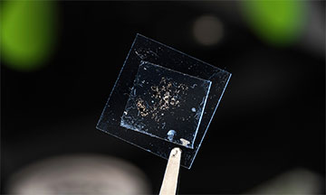
Researchers can process 100 images covering 1 cm×1 cm-sized samples like the one shown in the photo in around nine minutes using a new system that greatly simplifies the often-tedious search for monolayers in the lab. [Image: J. Adam Fenster, University of Rochester]
Scientists require monolayers—graphene and other 2D materials—to detect, emit and modulate signals within integrated-photonic devices. Distinguishing between true monolayers and other thin films, however, requires hours of tedious human examination, during which the precious 2D materials can degrade.
But researchers in the United States and Mexico have simplified the time-consuming quest by enlisting deep-learning algorithms to handle the painstaking work (Opt. Mater. Express, doi: 10.1364/OME.454314). The combination of digital-image processing, an inexpensive microscope and camera setup, and the intelligent algorithm can detect true monolayers at a rate of 9 min/cm2, with a claimed accuracy rate of 99.9%.
Materials for photonic structures
Transition metal dichalcogenides such as tungsten diselenide, molybdenum disulfide and hexagonal boron nitride have electric and optical properties that make them ideal for the next generation of active photonic devices. However, picking out the true monolayers from multilayers takes human workers several hours, and humans can get tired and make mistakes. In addition, other workers must use a second technique such as atomic force microscopy or Raman spectroscopy to confirm the monolayer candidates.
Since many university-based researchers employ undergraduate students to search for monolayers, the process can extend over several days depending on the students’ availability, says Jaime Cardenas, an optics professor at the University of Rochester, USA. Meanwhile, the monolayers themselves can degrade during examinations, resulting in fewer square centimeters of pristine material to add to photonic devices.
Simple setup, advanced algorithm
Cardenas, whose Rochester laboratory focuses on nanoscale optical devices, says that one of the engineering graduate students who joined his group, Jesús Sánchez-Juárez, brought with him a background in deep learning. “We thought it would be a great application of deep learning to try to detect the monolayers automatically without having a person spend hours on the microscope,” Cardenas adds.
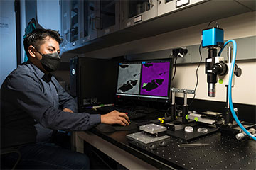
Jesús Sánchez-Juárez, a Ph.D. student at the University of Rochester, has developed a system—combining a microscope with a 5× objective lens, a low-cost camera and an artificial neural network—that dramatically speeds up and simplifies the process of detecting true monolayer materials. The materials are highly sought after for use in electronics, photonics and optoelectronic devices. [Image: J. Adam Fenster, University of Rochester]
The two researchers, along with Rochester optics graduate student Marissa Granados-Baez and professor Albert A. Aguilar-Lasserre from the Instituto Tecnológico de Orizaba, Mexico, designed a digital-imaging setup based on a basic microscope with a 5× objective lens and camera. The setup passed images through several filters to maximize the contrast between the monolayer and the background surface. A white-balance correction plus noise reduction increased the distinction between colors in the resulting series of images.
Next, the filtered images were fed into two sequential deep-convolutional neural networks, which extracted target characteristics from an initial data set and then identified similar targets in succeeding images. Collecting the 580 images to train the first of the two networks took about 200 hours of work, according to the researchers.
The biggest challenge in the effort, according to Cardenas, was finding an image-processing algorithm that would provide a consistent baseline sample for training the neural network. For the deep learning, the group turned to AlexNet, an influential neural-network architecture developed about a decade ago.
Deep learning for integrated photonics
Cardenas says his group will continue to use deep learning to accelerate integrated-photonics manufacturing and packaging. He adds, “Our undergrads do more interesting things now, such as stabilizing a laser with a cavity, measuring the second-order coherence of light or building setups to test the temperature stability of our devices.”