
Researchers have developed an all-optical method for driving multiple high-density nanolaser arrays using light traveling down a single optical fiber. The optical driver creates programmable patterns of light via interference. [Image: M.-K. Kim, Korea University] [Enlarge image]
As integrated circuitry moves from the electronic to the photonic realm, real estate on increasingly miniaturized chips becomes scarce. Yet arrays of nanoscale lasers have required pairs of electrodes for pumping, taking up lots of that precious space, as well as devouring energy and creating information bottlenecks.
Now a research team based in the Republic of Korea has demonstrated an all-optical pumping method for driving arrayed nanolasers spaced just 18 μm apart (Optica, doi:10.1364/OPTICA.471715). The technique could boost new applications for tiny lasers in photonic chips and quantum networks.
Shrinking photonic-chip sources
Optical scientists have long known that photonic circuits can leverage wavelength division multiplexing (WDM) to raise operating bandwidth by an order of magnitude or more above that of electronic systems. Even the tiniest lasers in a working array, though, have needed comparatively bulky electrodes to provide power; researchers had relegated optical pumping to testing small lasers.
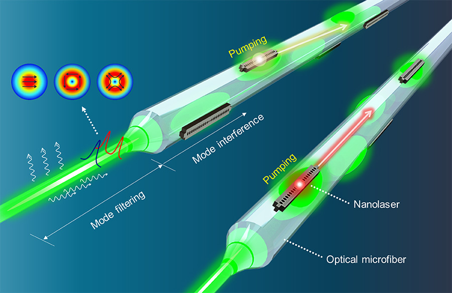
To demonstrate optical array pumping experimentally, a team at Korea University first heat-stretched and tapered a standard single-mode glass fiber. In its narrowest mode-filtering region, the length of optical fiber had a diameter of only 1.2 μm, whereas in the wide-diameter section 2.0 μm across, the modes that made it through the narrow region created interference patterns to pump the nanolasers.
The researchers fabricated three tiny lasers—dubbed photonic-crystal nanobeam (PCN) lasers—on an indium gallium arsenide phosphide wafer, and transferred the lasers to the outer surface of the tapered fiber. “This allows the light traveling through the fiber to be optically coupled with the lasers attached to the fiber surface,” says team leader Myung-Ki Kim, an engineering professor at Korea University.
Micro-alignment
In the experiments, the beam from a pulsed 976-nm-wavelength laser passed through a polarization controller and into one end of the optical fiber. The single-mode lasing output from the PCNs came out both ends of the fiber, but the researchers analyzed only the beam exiting from the end opposite the pulsed laser. An infrared CCD camera captured images during the experiments.
The researchers fabricated three tiny lasers—dubbed photonic-crystal nanobeam (PCN) lasers—on an InGaAsP wafer, and transferred the lasers to the outer surface of the tapered fiber.
Pumping and programming multiple small lasers or laser arrays through a single pump line, rather than multiple pump lines, would have been impossible with the conventional method of pumping the arrays with electron through a copper wire, Kim says.
The key to validating the results, as well as the team’s biggest challenge, was the 3-D fine alignment of the three PCNs on the surface of the optical fiber according to the interference pattern of the pump beam, Kim says. The team had to develop a high-resolution micro-transfer printing technique to fabricate the nanolasers on a III-V semiconductor wafer, then detach them with a confocal microscope and a micron-sized polydimethylsiloxane (PDMS) stamp. The group used two high-precision positioning stages to place the nanolasers 18 μm apart along the stretched fiber.
Programming the nanolaser arrays
According to Kim, programming the optically pumped nanolaser array is conceptually different from the electronic-array version of the task. In the latter, copper electrodes deliver electrons to each individual laser point-to-point. The Korea team’s method, in contrast, employs the interference pump beam through a single optical fiber or waveguide to drive and program multiple lasers from a single source.
“This technology can also be applied to chip-based silicon photonics systems, which could play a key role in the development of chip-to-chip or on-chip optical interconnects that are critical components for next-generation data centers,” Kim says. “In order to apply our all-optical laser driving and programming technology to silicon photonics, it is necessary to prove how independently the modes of a silicon waveguide can be controlled.”
The research team included two scientists from the University of California Berkeley, USA, where Kim is a visiting professor.