
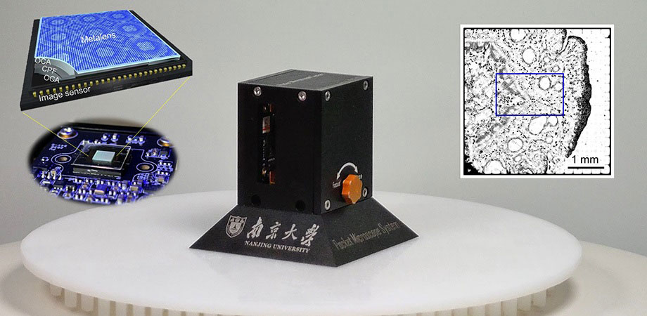
A chip-scale metalens array makes a microscope system ultracompact. [Image: T. Li, Nanjing University] [Enlarge image]
Traditional optical microscopes contain refractive optical elements that are ill-suited to miniaturization. One possible approach to developing ultracompact, lightweight microscopes is the metalens, a flat, wafer-thin chip composed of subwavelength units that can manipulate light.
Now, researchers from Nanjing University, China, have created a chip-scale metalens microscope with simultaneous large field-of-view (FOV) and depth-of-field (DOF) (Adv. Photon., doi: 10.1117/1.AP.4.4.046006). The device exceeds the performance of conventional microscopes with the same resolution, while allowing for an impressive thousand-fold reduction in volume and weight.
Improving on a prototype
Metasurfaces, which manipulate light with subwavelength unit cells, have the advantage of ultrathin and flat architectures. In 2020, Tao Li, senior author of the new paper and principal investigator at Nanjing University’s National Laboratory of Solid-State Microstructures, and his colleagues reported on their initial version of a metalens-integrated compact imaging device for wide-field microscopy. While it was small in size and expanded the FOV without sacrificing resolution, the prototype had relatively poor imaging quality due to its low efficiency with background noise.
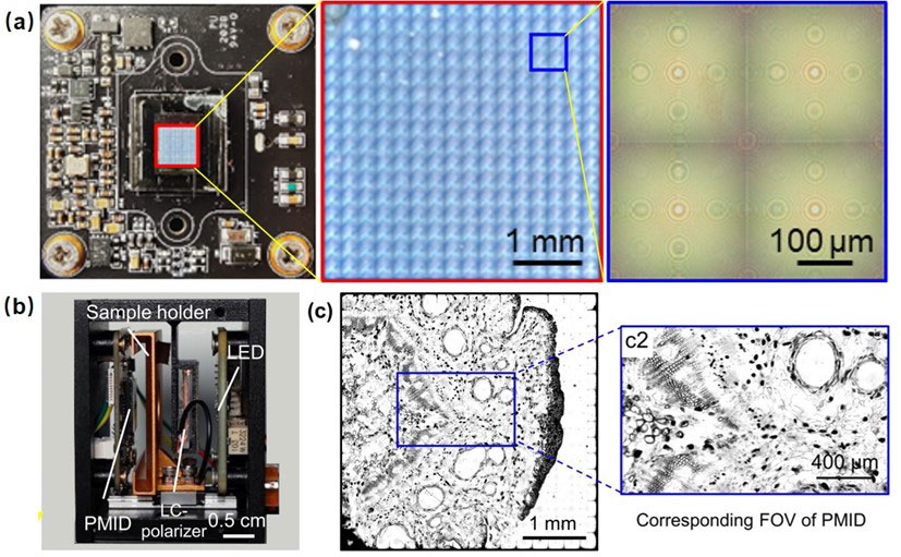
Chip-scale metalens array for polarization-embedded metalens imaging device (PMID) and compact portable microscope system (PMS). Top: a photo of the chip-scale PMID (left) and images of chip-scale metalens array integrated in the CMOS image sensor (middle and right). Bottom left: the PMID, sample holder, liquid-crystal polarizer and LED source are packed into the PMS with a compact size of 3×3.5×4 cm3. Bottom middle and right: wide-field microscopic image of a pine stem cross-section covering a 4×4-mm2 FOV with 1.74-μm resolution. The blue box indicates the recorded FOV of a traditional microscope. [Image: Ye et al., doi 10.1117/1.AP.4.4.046006] [Enlarge image]
The current study describes the researchers’ efforts to improve the microscope’s performance. The polarizer-embedded metalens imaging device (PMID) is based on geometric silicon nitride metasurfaces directly mounted onto a complementary metal-oxide semiconductor (CMOS) image sensor. In particular, the researchers added a fixed circular-polarization filter that is sandwiched between the metasurface and CMOS, affixed by a layer of optically clear adhesive tape on either side.
The metalens modulates the co- and cross-polarized light independently, enabling the embedded circular polarization filter to work for both orthogonal polarization illuminations to construct two sets of subimages. These subimages are then stitched together to form a single high-quality, wide-FOV image. As a result, the chip-scale PMID has a resolution of 1.74 µm and a FOV of 4 mm×4 mm.
“To the best of our knowledge, this is the first time a metalens imager has accessed a larger FOV than a traditional microscope with similar imaging quality,” said Li, in a press release accompanying the work.
Depth-of-field imaging
In addition, the broadband property of the metalens allowed for large-DOF imaging by tuning the illumination wavelength. Li and his colleagues employed the PMID to image different biospecimens, such as human umbilical vein endothelial cells in solution. They tuned the wavelength from 450 to 510 nm to derive DOF information stemming from the spectral zooming effect, and the DOF was measured to be approximately 200 µm.
“By sweeping the illumination wavelength, the device is able to achieve large-DOF imaging simultaneously, thanks to the large dispersive nature of the metalens,” said Li. “This chip-scale PMID enables the implementation of miniaturized portable microscope system.”