
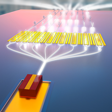
A US-based team has demonstrated a method for integrating high-power, electrically pumped DFB lasers onto a lithium niobate LN chip—and built a prototype transmitter by combining these lasers with LN electro-optical modulators. [Image: Second Bay Studios/Harvard SEAS]
The material lithium niobate (LN) has earned its stripes for decades as a platform for electro-optic modulators (EOMs)—the gadgets that convert signals from the electrical to the optical domain in optical communications systems and other signal processing and sensing applications. And the past five years have seen huge strides in miniaturizing these devices to the chip scale, using LN thin films.
Yet to do their magic in real-world systems, these nifty chip-scale devices still need to be hooked up to external lasers, to give the EOMs a source of light to modulate. And the costs and complexities of coupling these discrete components has held back progress toward scalable, fully integrated LN systems that could advance not only telecom applications, but also other areas such as spectrometry, lidar and remote sensing.
A team of US-based researchers has now demonstrated a clever, potentially scalable approach toward squeezing tiny, powerful and electrically pumped distributed-feedback (DFB) lasers onto a thin-film LN chip (Optica, doi: 10.1364/OPTICA.448617). Using this approach, the team was able to fashion on-chip integrated lasers that could push up to 60 mW of optical power into thin-film LN waveguides. Further, as a proof of concept, the researchers also put together a prototype high-power transmitter that combined such a DFB laser with a 50-GHz integrated EOM fashioned in thin-film LN.
Lasers wanted
LN excels as a modulator material in large part because it supports a strong Pockels effect—that is, rapid, substantial changes to the material’s optical properties in response to a small applied electric field. Before the mid-2010s, however, shrinking these blazing-fast, power-efficient modulators down to chip scale had been tough to impossible, owing to fundamental challenges in etching waveguides into bulk lithium niobate.
In 2018, a team led by Optica Fellows Marko Lončar of Harvard University and Peter Winzer of Nokia Bell Labs overcame those problems by turning to a relatively new option: LN thin films. By laying down a 600-nm-thick single-crystal LN film atop a CMOS-compatible substrate, the team was able to dry-etch low-loss LN waveguides and subsequently to demonstrate an integrated lithium niobate EOM that was 100 times smaller and 20 times more efficient than the fountain-pen-sized modulators then common on the market.
A natural next step was to find a way to integrate lasers into this new, smaller LN package, which would open the door to integrated transmitters—and, potentially, a range of other powerful chip-scale devices. In work published last October, a team led by Bart Kuyken at Ghent University–imec, Belgium, demonstrated one approach toward such integrated lasers: micro-transfer printing of integrated optical amplifiers, made of III–V materials, directly onto LN waveguides. The approach enabled the team to demonstrate single-mode lasing on an integrated LN base—but the maximum output power recorded from this laser was a relatively low 0.77 mW.
Flip-chip approach
Lončar’s team at Harvard, along with colleagues at the US firms HyperLight (which Lončar cofounded) and Freedom Photonics, has now demonstrated a different approach to integrating lasers into LN waveguides. The researchers focused on direct coupling of integrated DFB lasers—already well established in the industry for their small footprint, low cost and high output powers—with integrated LN waveguides. To link up those two components on one common platform, Lončar said in a press release accompanying the research, the team “used all the nano-fabrication tricks and techniques learned from previous developments in integrated lithium niobate photonics.”
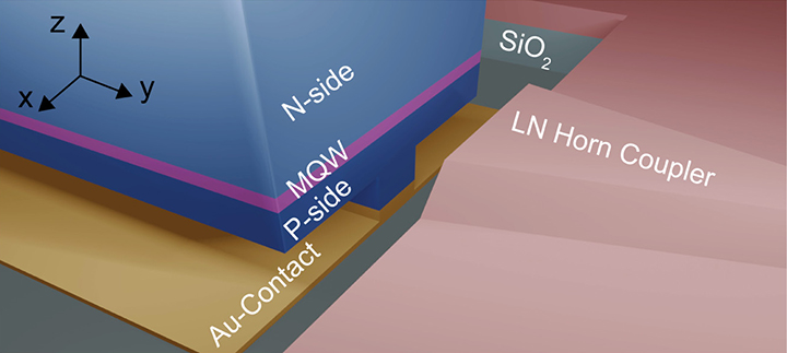
In the Harvard team’s approach, an integrated on-chip DFB laser (left) is flipped and bonded onto a gold electrode opposite a flared lithium niobate (LN) waveguide. The thickness of the gold layer can be varied to optimize mode-height matching between the laser and the LN waveguide, and thus to minimize power loss at the coupling. [Image: A. Shams-Ansari et al., Optica, doi: 10.1364/OPTICA.448617 (2022)] [Enlarge image]
The approach begins with a 600-nm-thick LN thin film device layer, which is bonded onto a 4.7-µm-thick SiO2 layer that sits on a silicon substrate. The 800-nm-wide waveguides etched into the LN device layer are flared out to a width of 8.2 µm at the planned point of coupling with the DFB lasers. This “horn” coupling geometry, the team writes, “ensures maximal overlap with the optical mode produced by the 5-µm-wide DFB laser”—and also enables a margin of safety against various kinds of potential misalignment.
At the end of the horn coupler, perpendicular to the LN waveguide, a trench is then dug out of the LN and SiO2 layers, using reactive-ion etching, to accommodate the butt-coupling of the DFB laser, built on a separate chip. The DFB laser chip is flipped and planted, directly opposite the flared waveguide, onto a gold bonding layer, which also serves as one of the electrodes of the electrically pumped laser.
Crucial to making this setup work is careful matching of the mode height in the DFB laser with that of the LN waveguide, to ensure the maximum coupling of single-mode optical power. The team accomplishes this using an ingeniously simple control knob: simply fine-tuning the thickness of the deposited gold layer until the mode-height matching is optimized.
High power for multiple applications
Using this method to couple integrated DFB lasers to passive integrated LN waveguides, the Harvard-led team achieved estimated on-chip output powers on the order of 60 mW (at a 1.0-A driving current)—which, the authors write, “is among the highest reported for all integrated photonics platforms.” The team also assembled a proof-of-concept application in which DFB lasers were integrated with a 50-GHz EOM in thin-film LN to create an electrically pumped, integrated laser transmitter. For these active devices, the output power (at a 0.8-A driving current) was a lower 25 mW, which the team attributes to suboptimal alignment in the prototype and to details of the modulator design.
The research team believes that the fabrication approach and the prototype transmitter platform it demonstrated enable “a new class of applications in digital and analog communications spaces.” But the team also sees a range of opportunities in other areas. For example, combining laser integration with integrated ring-resonator and Kerr frequency combs—where LN thin films have also made significant recent inroads—could represent “a critical step,” according to the team, toward fully integrated spectrometers. And other openings to leverage the technique, the authors suggest, may exist in remote-sensing and beam-forming systems, and in photon-pair generation and frequency conversion for quantum communication networks.
“It’s a building block,” first author Amirhassan Shams-Ansari, a grad student in Lončar’s lab, said in a press release, “that can be integrated into larger optical systems for a range of applications, in sensing, lidar, and data telecommunications.”