
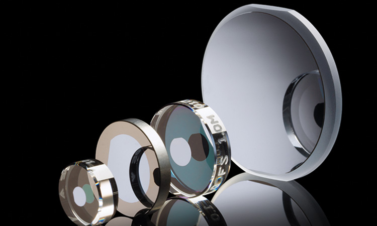
 Semiconductor supermirrors employing GaAs/AlGaAs multilayers directly bonded to various substrate materials including fused silica, SiC and sapphire. These structures are a specific class of the general CSOI platform, with sizes now ranging from 12.7 to 200 mm in diameter. [Thorlabs Crystalline Solutions]
The microelectronics revolution was built on a foundation of monocrystalline silicon wafers, the platform on which nearly all integrated logic devices have been fabricated. And advances in semiconductor manufacturing, as well as the availability of high-purity and high-structural-quality base materials, have enabled significant progress in advanced photonics.
One particular extension of traditional microelectronics technology, so-called silicon-on-insulator (SOI) wafers—originally developed some 30 years ago for high-voltage switching and microwave devices—has emerged as an indispensable tool for modern optics. SOI wafers, rather than relying on a continuous bulk silicon structure, consist of a thin layer of crystalline silicon transferred onto an oxidized silicon handle substrate. The platform’s compatibility with CMOS infrastructure has allowed commercially available photonic integrated circuits (PICs) to be realized on SOI wafers, and scaled up to 300-mm diameter for high-volume production.
The compound semiconductor on insulator (CSOI) platform has the potential to enable radically new devices with enhanced performance.
Yet, successful as SOI has been, the field is ripe for advancement. Beyond silicon, there is a spectrum of alternative crystalline materials—compound semiconductors, an important subset of which are formed from combinations of Group III and Group V elements on the periodic table. As we discuss in this feature, novel combinations of III–V materials and insulators, integrated onto low-index base material—a platform that we call compound semiconductor on insulator (CSOI)—have the potential to enable radically new devices with enhanced performance. The devices range from surface-normal optical interference structures for precision metrology, to high-performance transceivers relevant to datacom applications, to, ultimately, nonclassical light sources that will power the next generation of integrated quantum photonic technologies.
From SOI to CSOI
A key advantage of SOI is its ability to integrate high-quality crystalline films on effectively arbitrary base materials. As these structures rely on separate crystal growth and bonding, integration of the crystalline film is not limited by constraints imposed by crystal growth (such as lattice matching, which requires compatible unit cell symmetry and inter-atomic spacing).
Moreover, SOI can realize a large refractive-index difference between the transferred silicon and insulating underlayer. In optics, such a high index contrast enables enhanced flexibility in manipulating light’s wave nature. This brings several advantages in surface-normal optical-interference devices, such as a reduced field penetration and wide-bandwidth operation, which also holds in spatially patterned metasurfaces and grating-based devices. Similarly, in integrated photonic systems, a high index contrast leads to strong mode confinement, which makes SOI PICs more compact than devices on “native” substrates with a more limited index contrast.
Yet III–V materials open up considerably richer opportunities. Via hetero-epitaxy and band-gap engineering, multilayers of various crystalline films can be realized that have tailored optical properties far beyond what can be realized in single-layer SOI. Epitaxial III–V materials can have optical losses rivaling those of optimized dielectrics, making for excellent passive elements such as interference coatings and waveguiding structures. And unlike silicon, whose refractive-index-tuning opportunities are limited, varying the composition of ternary and quaternary alloys of arsenide-, phosphide- and nitride-based III–V materials allows for the modulation of the index profile of the thin films—all while retaining the performance advantages of single crystalline films.
While silicon is an excellent microelectronic material and passive photonic platform, III–V semiconductors enable active electro-optic functionalities. Bulk silicon has an indirect band gap and thus cannot be used for efficient light emission or optical gain. Its nonlinear properties are also wanting. For example, the lack of a second-order nonlinearity or Pockels effect prevents the realization of efficient frequency converters or high-speed modulators on SOI. The relatively low band-gap energy (~1.1 eV) of silicon also leads to high nonlinear loss (two-photon absorption, or TPA) for telecommunications and mid-infrared (mid-IR) wavelengths, which is essential for nonlinear optics such as frequency-comb generation.
Combining epitaxial growth of compound semiconductor structures with crystalline layer transfer techniques therefore allows for the development of advanced photonic devices, reaching far beyond the current capabilities of SOI-based structures. In the rest of this feature, we look at the potential advantages of this platform in a variety of integrated-photonic devices and contexts.
 The foundation of CSOI—wafer bonding of compound semiconductors made from the highlighted elements in the periodic table to insulating substrates—creates a wide application space. [Photos: Getty Images]
CSOI in surface-normal photonics
The earliest published example of a CSOI device stretches back nearly 50 years, to the demonstration of GaAs/AlGaAs-on-glass photocathodes developed at Varian in 1975. These novel optoelectronic structures sought to overcome limitations associated with the limited optical transparency of a native GaAs growth wafer. When direct deposition on non-lattice-matched, wide-band-gap semiconductors such as GaP proved problematic, the researchers chose to fusion-bond the epi films to a transparent glass substrate.
Over the ensuing decades, numerous international efforts focused on layer transfer and direct bonding for the heterogeneous integration of III–V materials on arbitrary substrates, with a notable example being work by Eli Yablonovitch and colleagues in 1990. This foundational work led to continued development of a diverse suite of heterogeneously integrated devices, spanning evanescent hybrid III–V silicon optoelectronics to high-brightness LEDs on transparent substrates and now to stamp-mediated processes for combining nanoscale compound semiconductor materials with traditional microelectronics.
By the early 2010s, CSOI enabled a unique solution to limitations in surface-normal photonics. These devices—developed by Garrett Cole, then at the University of Vienna, Austria, and later commercialized via the firm Crystalline Mirror Solutions—consist of GaAs/AlGaAs-based distributed Bragg reflectors that are separately grown and then transferred to super-polished fused silica substrates. In this process, monocrystalline interference coatings are applied to arbitrary (including curved) optical surfaces.
These techniques can overcome a long-standing challenge in precision interferometry: thermal noise. Pioneering studies in the gravitational-wave (GW) community showed that Brownian noise—subatomic thermo-mechanical motion in an object—is a limiting factor in the ultimate sensitivity of phase-based position measurements, in turn setting the ultimate limit in displacement measurements. As with GW detectors, Brownian motion sets bounds on the minimum linewidth of the laser systems at the heart of optical atomic clocks. Thus, the same noise processes affect the world’s most advanced measurement devices in their quest to probe the ultimate limits of space and time.
The magnitude of the Brownian motion is ultimately driven by the excess mechanical dissipation in multilayer optical coatings. Over the past two decades, a concerted effort has focused on identifying materials that simultaneously exhibit ultralow optical and elastic losses. Though capable of minimal absorption and scatter, amorphous thin films, because of their imperfect, glassy nature, exhibit significant mechanical loss and, thus, Brownian noise. In contrast, crystalline solids, with their low elastic losses, are capable of reduced noise.
The core optics in both GW detectors and optical clocks require high-quality glass substrates (and in the case of the clock laser systems, they have relatively strong curvature). That makes them unsuitable for direct epitaxial growth. This is overcome via a layer transfer process that allows high-quality GaAs/AlGaAs multilayers to be integrated with super-polished fused silica substrates. The tenfold reduction in elastic losses from the resulting “crystalline coatings” can slash Brownian noise.
Initially there was some skepticism about the minimum achievable optical losses (scatter and absorption) in such semiconductor-based “supermirrors.” Yet, optimization of the crystal growth and layer transfer processes has led to the demonstration of crystalline coatings with performance metrics comparable to, or even exceeding, the best sputtered mirrors. Semiconductor supermirrors are now routinely produced with excess optical losses (scatter + absorption) at the few-parts-per-million level. Standard commercial products can be found with reflectances greater than 99.999% in the near-IR spectral region, enabling the construction of the world’s most stable interferometers.
Echoing the remarkable success of high-quality crystalline mirrors for free-space optics, CSOI structures can pack significant advantages for integrated photonics.
Efforts continue with the development of both room-temperature and cryogenic laser systems targeting mHz-level integrated linewidths. Parallel R&D activities focus on scaling the maximum coating diameter (currently at 20 cm) to sizes relevant to GW observatories. Aiming to extend the wavelength range of these coatings, mid-IR (center wavelength ~4500 nm) crystalline coatings exhibiting the lowest excess optical losses of any coating technology to date were demonstrated in 2021. At the opposite end of the spectrum, visible-wavelength mirrors targeting Sr clock and ring-laser gyroscope applications are currently under development. Beyond terrestrial uses, cavities employing crystalline mirrors have reached a technology readiness level (TRL) of 6, and are now space qualified for future satellite platforms.
The combination of epitaxial layer transfer with optimized optical substrates has thus allowed for the generation of CSOI-based surface-normal photonics with the highest performance yet constructed. Looking ahead, we see a bright future for crystalline coatings in applications requiring the ultimate levels of optomechanical and thermal performance.
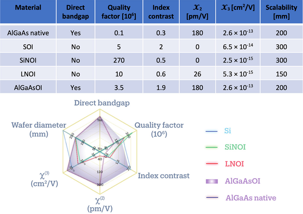 Key metrics for commonly used photonic platforms. [Data from M.W. Puckett et al., Nat. Commun. 12, 934 (2021), W. Jin et al., Nat. Photon. 15, 346 (2021), L. Chang et al., Nat. Commun. 11, 1131 (2020), and P. Kuo et al., Nat. Commun. 5, 3109 (2014)] [Enlarge graphic]
CSOI waveguides for integrated photonics
Echoing the remarkable success of high-quality crystalline mirrors for free-space optics, CSOI structures can pack significant advantages for integrated photonics. Compared with traditional III–V photonic structures grown on lattice-matched native substrates, CSOI structures exhibit a larger index contrast, which is essential for fabricating compact devices. CSOI also provides flexibility for tailoring the device geometry to engineer dispersion and optimize phase-matching conditions. Compared with SOI waveguides, CSOI supports richer optical processes such as optical gain, second-order nonlinearity, Pockels effect, piezo-electric effect and acousto-optic effect.
AlGaAs ternary alloys stand out among the wide range of III–V semiconductor candidates for integrated photonics. With optimized epitaxial growth processes and band-gap engineering, the intrinsic optical losses of these alloys can be low, while their transparency window can be wide (down to 574 nm). This enables TPA-free operation in the telecommunications band (1310 nm and 1550 nm). AlGaAs-based materials also exhibit extremely high second- and third-order nonlinearities—two essential optical properties for nonlinear photonics. And the material is already widely used in both photonics research and foundries, with mature growth and processing technologies that advance both platform development and long-term commercialization prospects.
The first successful attempt at building AlGaAs-based CSOI (AlGaAsOI) structures for integrated photonics was realized in 2016 by the team of Kresten Yvind at the Technical University of Denmark. In this work, a single AlGaAs layer was transferred onto an oxidized silicon substrate, similar to the methods used for high-quality crystalline mirror construction. To define the waveguide, the wafer is patterned by electron beam lithography, dry etching and cladding deposition. The final waveguide cross section comprises an AlGaAs core fully cladded with SiO2.
Although advantageous in many aspects, originally this platform was not regarded as a promising direction for integrated photonics due to the high waveguide loss—initially one order of magnitude higher than in SOI. This was the key bottleneck limiting the performance and scalability of III–V photonics.
This status quo was challenged by the team of John Bowers at the University of California, Santa Barbara, USA, in 2020, motivated in part by the low-loss GaAs/AlGaAs crystalline coatings demonstrated a few years earlier. By combining two strategies for loss reduction—the suppression of scattering loss and passivation of surface defects—the propagation loss of AlGaAsOI waveguides was reduced to the same level (less than 0.2 dB/cm) as the best SOI and many dielectric platforms. The desirable properties of III–V materials could thus be harnessed without the penalty of excess optical losses.
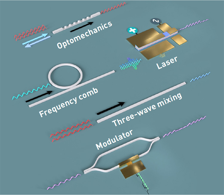 Versatile functions that can be achieved on AlGaAsOI platform include acousto-optical processes, Kerr comb generation, second-order frequency conversion, electro- optic modulation and electrically pumped lasers. [Enlarge graphic]
Nonlinear photonics: An efficiency leap
The successful demonstration of AlGaAs-based CSOI waveguides and a significant reduction of the limiting material loss have opened new opportunities and application spaces for integrated photonics. The impact has been immediate on nonlinear photonics. Because the second- and third-order nonlinearities of AlGaAs are both significantly higher than those of commonly used photonic materials, AlGaAs-based devices can boost the efficiencies of various nonlinear processes dramatically.
The first record-breaking nonlinear device demonstrated on CSOI was for second-harmonic generation (SHG) with a high-aspect-ratio waveguide geometry. The large index contrast allowed quasi-phase-matching to be achieved by leveraging the birefringence between the TE and TM waveguide modes to compensate the dispersion between fundamental and second-harmonic wavelengths. Combined with a giant χ(2) nonlinearity, a record high normalized SHG efficiency (45,000% W–1cm–2) was demonstrated—one order of magnitude higher than that demonstrated with linear waveguides in other material platforms.
Another crucial structure for nonlinear photonics—high-quality-factor (Q) microring resonators—can also be fabricated in low-loss AlGaAsOI. A Q up to 3.5 million has been successfully realized, comparable with many low-loss dielectric waveguides such as lithium-niobate-on-insulator or Hydex, but with much smaller mode size. Hence, the nonlinear efficiency can be further boosted by resonant light inside the cavity. Following this route, an optical frequency comb generated on AlGaAsOI microresonators, demonstrated in 2020, showed an unprecedentedly low pump power down to 20 µW, and hundreds of comb lines were attainable at less than 1 mW pump power.
The remarkable leap of nonlinear efficiencies afforded by AlGaAsOI should transform the field of nonlinear photonics in the years to come. The drastic reduction in pump power for on-chip nonlinear optics, combined with the fact that AlGaAs is compatible with direct laser integration, provides one promising route toward fully integrated nonlinear photonic circuits. AlGaAsOI also offers a broad transparency window, from 500 nm to 10 µm, that could support broadband nonlinear frequency conversion or supercontinuum generation in the mid-IR spanning more than an octave.
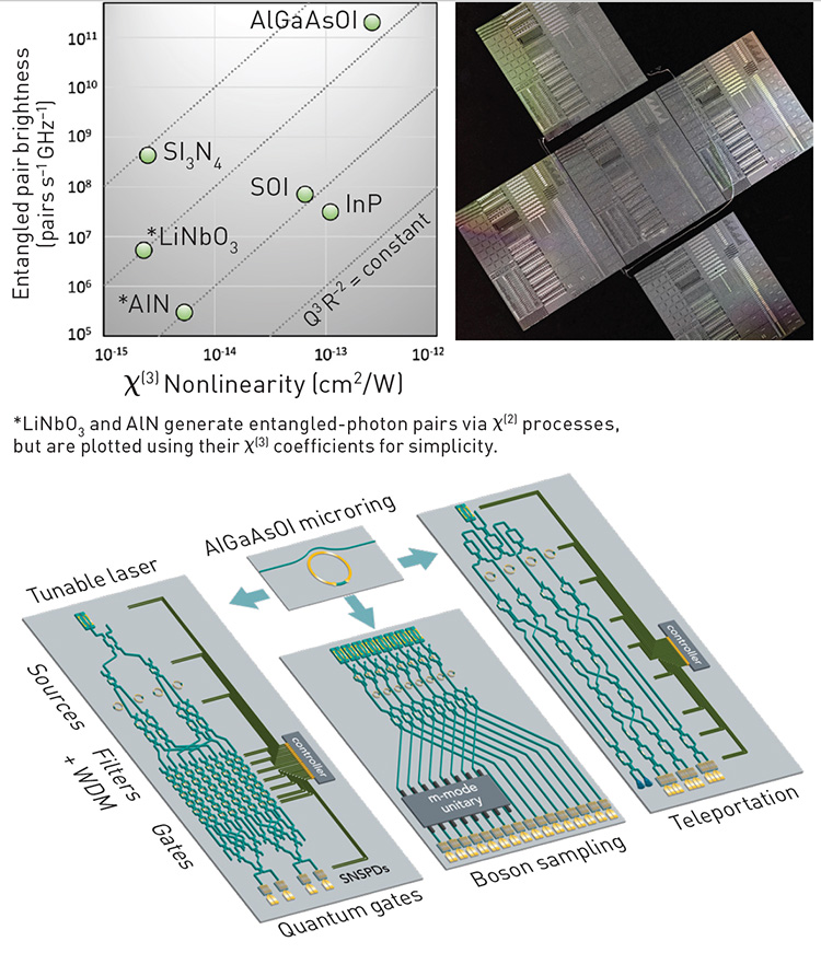 Top left: Entangled-photon-pair generation rate versus optical nonlinearity for various photonic platforms. Top right: Multifunctional integrated quantum photonic devices fabricated in AlGaAsOI, including tunable sources, tunable Mach-Zehnder interferometers, qubit demultiplexers and pulse shapers. Bottom: Illustration of all-on-chip quantum photonic circuits with integrated tunable pump lasers, quantum light sources, filters and demultiplexers, programmable logic gates and detectors. [Enlarge graphic]
From classical to quantum
While integrated photonics R&D has a long and rich history for classical technologies, the past decade has seen remarkable advances in quantum photonic integrated circuits (QPICs) and related applications. Already, QPIC development has seen key milestones including on-chip multiphoton interference and quantum logic gates, chip-to-chip quantum communications, QPICs for universal linear quantum optics and hybrid platforms with PIC-integrated trapped-ion systems.
Most of these approaches leverage the foundry capabilities of silicon photonics, with nearly a thousand components integrated on-chip for programmable quantum photonic networks. Yet, as QPIC complexity and functionality continue to evolve, silicon’s limitations are becoming increasingly apparent. Specifically, the material’s lack of suitable gain, telecom-wavelength photodetectors and other high-speed active components points to a future of hybrid QPICs that combine different materials in a monolithic, heterogeneous platform.
That potential future has spurred development of many alternative QPIC platforms, including silicon carbide, lithium niobate, diamond and III–V materials. It has become clear only in the past several years that CSOI could compete with silicon-based PICs for integrated quantum photonics.
In 2019, for example, researchers in Hong Kong and the Netherlands used a microring resonator fabricated in InP on benzocyclobutene (BCB) for generating telecom-wavelength time–energy-entangled photon pairs through spontaneous four-wave mixing, demonstrating a pair generation rate (PGR) of 145 MHz mW–2
—comparable to the rate obtained with SOI. This was achieved, despite a lower resonator Q than in SOI, owing to the larger third-order nonlinearity of InP—although InP still suffers from two-photon absorption, which places an upper bound on the PGR.
In 2021, researchers from Moody’s and Bowers’ group at UCSB demonstrated entangled-photon-pair generation from AlGaAsOI microring resonators with Q above 1 million. The combination of high Q, large third-order nonlinearity, negligible two-photon absorption and tight modal confinement resulted in nearly a thousand-fold improvement in the source brightness compared with SOI. Another approach under development by researchers at the Université de Paris and Sorbonne Université, France, leveraging the even larger nonlinear effect (χ(2)), has shown promising progress with 10 MHz off-chip PGR of polarization-entangled photon pairs from type-II spontaneous parametric down-conversion in AlGaAs ridge waveguides. Future designs combining the large second-order nonlinearity of III–V materials with the low loss and tight confinement of CSOI should yield further improvements in the efficiency while still maintaining the near unity Bell-state fidelity.
Finally, the large AlGaAsOI resonator Q corresponds to a waveguide loss of less than 0.2 dB/cm—comparable to the best performance from SOI and silicon-nitride waveguides designed for quantum photonic applications. This points to a bright future in multifunctional integrated quantum photonics with CSOI, which can naturally serve as a host for optical gain for tunable pump lasers, waveguide- and microresonator-based quantum light sources, integrated photodetectors and high-speed modulators, and programmable interferometric networks. The attributes that make CSOI compelling for entangled-photon-pair generation can also be leveraged for generating other nonclassical states of light with a similar performance in the generation rates and state fidelities—including squeezed light and deterministic single-photon emission from self-assembled quantum dots for continuous- and discrete-variable quantum information applications, respectively.
In the coming years, the transition of CSOI from small-scale efforts to volume production at semiconductor foundries will revolutionize the photonics ecosystem.
Outlook and perspective
With recent, rapid progress, CSOI holds the tantalizing prospect of revolutionizing photonics, by offering novel functionalities coupled with generally improved performance. The superior thermo-mechanical properties of crystalline coatings have already brought commercial uptake for them in surface-normal optical devices for precision interferometry and spectroscopy, high-power laser systems and more. Integrated CSOI devices have found use in parallelized light sources and signal processing in communications, and AlGaAsOI microcombs have enabled demonstration of reconfigurable RF filters for microwave photonics, offering promise for 5G/6G networking, radar and many other applications. Efficient microcomb sources on AlGaAsOI, combined with second-harmonic generation, could bring fully integrated time–metrology systems such as optical frequency synthesizers and compact atomic clocks.
Though AlGaAsOI is the focus of much R&D, we expect that the concept can be extended to other III–V and II–VI materials, including GaP, InGaP, GaN, ZnSe, ZnS and CdS. Wide-band-gap III–V semiconductors can lead to lower loss at visible wavelengths, benefiting many applications in atomic physics, biosensing and augmented and virtual reality. The large second-order nonlinearities and wider transparency window point to more efficient quantum light sources and PICs spanning a wide swath of the electromagnetic spectrum.
In the coming years, the transition of CSOI from small-scale efforts to volume production at semiconductor foundries will revolutionize the photonics ecosystem. We believe that this technology will dramatically extend the capabilities and scope of advanced photonics beyond current technologies, offering a powerful complement to SOI-based photonics.
Lin Chang, Galan Moody and John E. Bowers are with the University of California, Santa Barbara, CA, USA. Garrett D. Cole is with Thorlabs Crystalline Solutions, Santa Barbara, CA, USA.
References and Resources
-
G.A. Antypas and J. Edgecumbe. Appl. Phys. Lett. 26, 371 (1975).
-
E. Yablonovitch et al. Appl. Phys. Lett. 56, 2419 (1990).
-
G.D. Cole et al. Nat. Photon. 7, 644 (2013).
-
M. Pu et al. Optica 3, 823 (2016).
-
E.J. Stanton et al. Opt. Express 28, 9521 (2020).
-
L. Chang et al. Nat. Commun. 11, 1331 (2020).
-
W. Xie et al. Opt. Express 28, 32894 (2020).
-
G. Moody et al. J. Phys.: Photon., doi: 10.1088/2515-7647/ac1ef4 (2021).
-
R.R. Kumar et al. Appl. Phys. Lett. 114, 021104 (2019).
-
T.J. Steiner et al. PRX Quantum 2, 010337 (2021).
-
S. Ducci et al. Photoniques 107, 28 (2021).
For complete references and resources, visit: optica-opn.org/link/csoi.