
The devices that UCF researchers are developing will allow artificial intelligence to work from anywhere, without connecting to the internet. [Image: UCF]
Neuromorphic computing is a growing trend in computer engineering that uses the human brain and other body parts as inspiration to develop more efficient hardware and software. For instance, artificial visual systems consist of image sensors for detection, memory blocks to store data and processing units for pattern recognition and object identification.
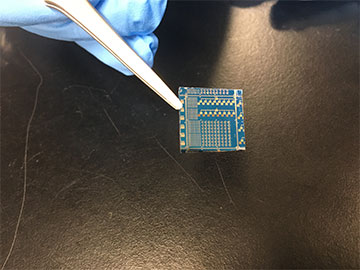
Now, researchers in the United States and South Korea have developed a multiwavelength optoelectronic synapse that allows optical data sensing, storage and processing to occur in the same device (ACS Nano, doi: 10.1021/acsnano.2c01035). The resulting in-sensor artificial visual system, which represents a significant advance in processing efficiency and image recognition accuracy, may have future applications in machine vision, self-driving vehicles and robotics.
Mimicking the human eye
Neuromorphic devices have the potential to overcome limitations of traditional artificial visual systems, which must sift through enormous amounts of redundant data to extract relevant information. However, current approaches still have image sensors, such as cameras and photodetectors, that remain physically separate from computing components. Such an arrangement can lead to system latency, bulkiness and added weight.
As a solution to this issue, the researchers created an all-in-one optoelectronic synapse that simultaneously operates in ultraviolet (UV), visible, near-infrared and infrared wavelengths of light. Previous studies have only demonstrated systems that can sense UV and visible light ranges.
“With our optoelectronic synapse, optical data sensing, memory and processing can be integrated in the same device—like the human eye, where optical data are sensed by the retina and memory and processing are done by the synapse and neurons,” says senior author Tania Roy, a materials and engineering professor at the University of Central Florida, USA.
A stack of 2D materials
Roy and her colleagues leveraged the versatility of 2D materials—which have the photosensitivity to act as image sensors, along with other unique properties needed for charge trapping—to build their device. In particular, they integrated the persistent photoconductivity of molybdenum disulfide with the wide absorption of platinum ditelluride to extend the device’s wavelength range.
The stack configuration of the optoelectronic synapse allows infrared light to pass through a top layer of molybdenum disulfide due to its high band gap. The light then gets absorbed by a platinum ditelluride film that sits underneath, resulting in a photogating effect. For UV and visible light, both layers generate electron-hole pairs and alter the device conductance accordingly.
Testing recognition accuracy
The researchers developed an artificial neural network to put the optoelectronic synapse to the test in a series of single-wavelength and mixed-wavelength pattern-recognition tasks. For example, the mixed-wavelength pattern consisted of an “8” with one half of the number in UV and the other in infrared. For datasets containing 800 test images with both single and mixed patterns, the researchers observed 70% to 80% recognition accuracy.
“Our multi-wavelength optoelectronic synapse has enormous potential in artificial intelligence, like autonomous vehicles and robotics,” says Roy. “The next step of the project is to build an artificial neural network with an array of devices [at the] hardware level to test and compare the pattern-recognition accuracy with the simulated results.”