
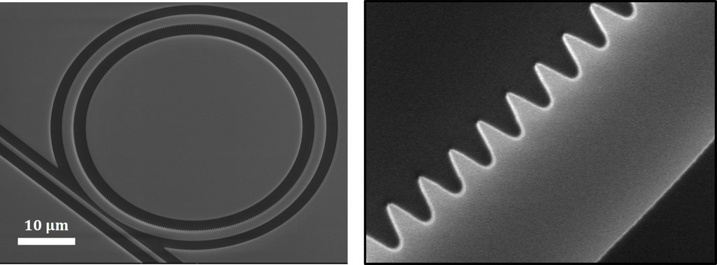
Scanning electron microscopy images showing the ring-shaped photonic crystal resonator (left), which features a nanopattern inside (right) that splits a selected resonant mode for comb generation. [Image: S.-P. Yu, NIST] [Enlarge image]
The already lightning-quick movement of information around data centers could become even quicker in the future thanks to a new kind of optical interconnect demonstrated by a multi-institutional collaboration in the United States. The link uses a novel photonic-crystal resonator and an inverse-designed waveguide structure to implement both wavelength- and mode-division multiplexing—carrying 40 channels that transmit 340 gigabits per second (Gbit/s) of error-free data (Opt. Lett., doi: 10.1364/OL.461272).
Improving data centers
Data centers operate by transferring vast amounts of information between numerous individual processors and memory banks at high speed. The interconnects used to establish these links can be exclusively electrical, but the higher frequencies and lower losses of light-based communication enable faster, more efficient transfers. However, optical interconnects currently require individual lasers for each data channel and thus consume significant amounts of energy.
In the latest work, a group led by Firooz Aflatouni at the University of Pennsylvania, Scott Papp at the National Institute of Standards and Technology (NIST), Jelena Vučković at Stanford University and Peter Delfyett from the University of Central Florida has shown how to merge two distinct kinds of multiplexing in one link, demonstrating very high error-free bit rates from a setup that could potentially be built entirely from integrated photonics.
Phase matching and multiplexing
The first half of the scheme involves a frequency comb made from a micrometer-scale ring of tantalum pentoxide with a free spectral range of 400 GHz. Frequency combs generate very brief pulses of light that in the frequency domain consist of a large number of narrow, equally-spaced “teeth.” They are usually devices that sit on an optical bench, but over the last decade or so, scientists have shown how they can instead be made from cavities measuring at most a few millimeters across (although they still require larger control electronics).
Generating frequency combs from such microresonators usually requires the resonators to display anomalous dispersion, meaning that their refractive index goes down as the frequency of incoming light goes up. Being able instead to exploit normal dispersion would improve efficiency and flatten out the comb’s spectrum, but the phase matching needed to produce the four-wave mixing for comb generation is usually not possible in this regime.
Papp and colleagues at NIST have shown how this can be done by etching the inner edge of the ring so that it forms a very shallow sine wave. Although just a few tens of nanometers from peak to trough, this pattern creates a photonic bandgap in one of the ring’s resonant modes. The gap splits the mode in two, such that the lower frequency part can be pumped to satisfy the necessary phase-matching condition.
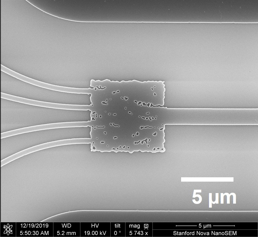
The researchers designed and optimized a mode-division multiplexer (shown in the image) that transforms each of the 10 wavelengths into four new beams that each have different shapes. This fourfold increase in data capacity creates 40 channels. [Image: K. Yang, Stanford University] [Enlarge image]
At the same time, Vučković and coworkers at Stanford have designed and built a new device to carry out mode-division multiplexing. The device creates multiple data channels by multiplexing light from four 500-nm single-mode waveguides into multimode light (with multiple, orthogonal orientations of the electric field) within a single 1800-nm-wide waveguide at input, and then demultiplexing it back into single-mode waveguides at the output. Each of the four channels separately contains all of the channels created via wavelength-division multiplexing.
Fast and error-free
The researchers made the multiplexer and demultiplexer by etching very precise patterns in 220-nm-thick layers of silicon sitting atop an insulator. They worked out these non-intuitive distributions of permittivity using a type of inverse design involving the iterative calculation of gradients to match up device structure with the desired output—allowing them to maximize the device’s efficiency while keeping it small.
To demonstrate the two devices together, the researchers pumped the frequency comb with a continuous-wave laser, selected just ten of the resulting frequency channels and lumped those into two groups in order to demonstrate simultaneous encoding with a pair of intensity modulators operating at 10 Gbit/s. Combining the two data channels (while introducing a delay between them), amplifying them and splitting the power into four different outputs, they then passed the signals through the mode-division multiplexer and demultiplexer before measuring the output with a photoreceiver and two amplifiers.
Using an analyzer to measure the frequency of errors, the researchers found that, for 34 of the 40 channels, fewer than one in a trillion (1012) of the transmitted bits had the wrong value. While those channels were considered “error-free,” the remaining six channels—with error rates of up to 1 in 10 billion—were not. The upshot was an overall transmission rate of 400 Gbit/s and an error-free transmission rate of 340 Gbit/s.
Boosting performance
Lead author Chinmay Shirpurkar of the University of Central Florida points out that this is not a record for transmission rates within data centers, explaining that the work was instead “more about the potential of using these compact novel integrated devices.”
Indeed, according to Shirpurkar, the collaboration is looking at a number of ways to boost performance in the future. He says that he and his colleagues have designed multiplexer-demultiplexer layouts that can accommodate 8 or 12 different spatial modes and are currently testing the performance of these structures. They are also designing integrated wavelength-division-multiplexing chips and modulators to replace the commercial devices used in the current experiment—which, he says, means they ought to be able to multiplex around 40 comb channels.
But first, Shirpurkar says they need to test their scheme using multimode fiber rather than a waveguide. This will allow them to measure the degree of cross-talk between channels and the amount of environmental noise likely to occur in a real-world setting.