
![]()
[Image: Metalenz]
In the past decade, academic research labs have published increasingly dazzling results demonstrating the rich potential of metasurfaces. These planar materials, decorated with collections of nanostructures and nanopatterns, can shape and direct light in intricately engineered ways, doing the heavy lifting of multiple optical components in a single 2D surface.
In principle, these accomplished engineered surfaces could radically reduce system size and complexity in a range of applications. But impressive as they’ve been in the lab, the use of metasurfaces in actual commercial devices has always seemed just out of reach—something that would happen at some point in the future, perhaps, but not quite today.
Now Metalenz—an early-stage company spun out of the research group of Optica Fellow Federico Capasso at Harvard University six years ago—says it has crossed that threshold. In early June, the company announced that its flat-lens “meta-optics devices” are now included in the VL53L8 direct time-of-flight (dToF) sensor produced and marketed by ST Microelectronics, a semiconductor manufacturer that’s a market leader in 3D-sensing modules. The Metalenz technology replaces multiple optical elements in existing ST ToF modules, which have been widely marketed to end-user applications in smartphones, drones, robots and vehicles.
In a press release, Metalenz said that this constitutes “the first time metasurface technology is commercially available and being used in consumer devices.” In an interview with OPN, Rob Devlin, the company’s co-founder and CEO, said that ST modules with Metalenz technology will be in consumer devices within the next several months. “To me, that’s one of the most exciting parts,” says Devlin. “The fact that it’s going to have a direct impact on end users, and not just a smaller market.”
From grad school to startup

Rob Devlin. [Image: metalenz.com]
Devlin himself got involved with Metalenz as a result of his Ph.D. work in Capasso’s lab in the early 2010s. In that work, he focused on improvements to performance and manufacturing of metasurfaces, to “get them to the point that they could really be useful for practical applications.” He was a coauthor on, among other studies, a landmark 2016 cover article in Science reporting a metalens that could achieve diffraction-limited focusing and subwavelength-resolution imaging across a range of visible wavelengths.
Up until that point, Devlin had been thinking mainly of an academic career. But after the appearance of the Science paper, he says, with “the amount of cold calls we started getting from cellphone manufacturers, from everyone in the optics industry, from entrepreneurs and investors asking us what we’re going to do—we said, ‘Well, I think it’s probably time now to see if this can be more than nice papers and research.’ ” So, in 2016, the company was spun out, with Devlin in the role of founder and CEO. And, he told OPN, “we’ve been working to find out where the technology actually will fit first ever since then.”
A focus on scalability
Part of that quest, says Devlin, is about developing systems that make metasurface devices manufacturable at scale. One of the promises of metasurfaces, he notes, has been that they can in principle be fabricated using the standard lithography techniques of the semiconductor foundry. But making that work in the real world requires going from a lab mentality, which focuses on “getting the five devices that are the best-performing ones,” to a commercial mentality in which millions of devices can be manufactured. In the latter case, what’s important is not necessarily peak performance; instead, it’s logging a sufficiently high, dependable average performance for the application in question.
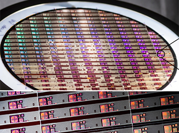
A wafer with multiple Metalenz metasurfaces (top) and a detail of the wafer (bottom). [Image: Courtesy of Metalenz]
Metalenz has thus focused on building design tools that could identify critical parameters for the metasurface to control in a given application, and that would optimize those parameters for “something that is going to be launched at scale,” according to Devlin. “It can’t just be, ‘Give me that golden sample that makes a perfect image,’ ” he says. “It has to be, ‘Okay—this is now going to be in millions of devices.’ ”
Unlocking a “completely new” approach
That focus on manufacturing processes and scalability underlies the recently announced milestone with ST—the result of a partnership originally announced roughly a year ago. The semiconductor maker’s FlightSense ToF module, in which Metalenz’s metasurface technology will replace existing optical elements, has sold more than 1.7 billion units to date. “The partnership of Metalenz IP with ST manufacturing technology,” according to a Metalenz release, “brings the incredible accuracy and precision of electronics chip industry to make very precise and repeatable meta-optics that unlock this completely new way to make lenses that combine very high quality and large-scale cost-effective manufacturing.”
“What ST has seen,” Devlin told OPN, “is the value of what we can do with metasurfaces, and what metasurfaces can do.” That value, he continues, lies in “reducing the overall complexity of an optical system,” and embedding the function of multiple “completely distinct and different optical devices” in one planar layer. ST “really saw how metasurfaces could make sure that they could push their module performance forward without adding more complexity to the overall system.”
Eyeing the longer term
Metalenz closed a US$10 million series A funding round with a number of strategic investors from the semiconductor industry in September 2020. The company now has a staff of 22 persons, according to Devlin, and is eying a series B round to further commercialize its offering. And Devlin says Metalenz is thinking well beyond early applications in 3D sensing and visible-light imaging, for which he characterizes metasurfaces as “a drop-in solution simplifying existing systems.”
In the longer term, by contrast, the company is looking at “designing full systems and modules around the unique capabilities of the metasurface,” which Devlin views as a platform technology. “There’s so much more you can do with metasurfaces,” he says. “You’re controlling light at such a fine scale, and you have control over all of the properties in light.”
Indeed, one item of particular interest to Metalenz—and announced at the beginning of 2022, with the unveiling of the company’s “Polar Eyes” technology—is the ability of metasurfaces to detect polarization information in light, which could open up a variety of new application areas for these compact surfaces.
“3D sensing and visible imaging are really interesting applications in cellphones today,” says Devlin. “But when you step back and think about it, those are actually things that human vision systems are already doing … [The] idea of being able to bring a new information [such as polarization] to people or to devices that we’re not seeing as humans today is, to me, one of the most exciting parts, and [something] we’re starting to push into products.”