
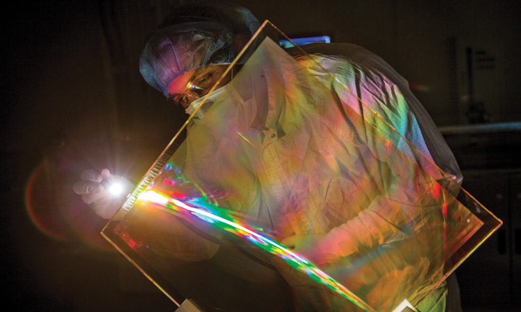
 Marcus Monticelli at the LLNL National Ignition Facility (NIF) inspects the antireflective coating on a NIF grating debris shield. [LLNL/J. Laurea]
Very soon after the advent of lasers in the 1960s, one major direction of development involved lasers that could deliver ever-higher energies to a target, to achieve electric-field strengths exceeding those binding electrons and nuclei. The goal was to study high-energy-density plasmas in controlled conditions within the laser’s focal volume. With this approach, such plasmas could be produced and studied without the need for uncontrolled above-ground or underground nuclear explosions.
 The 75-cm forward-optical assembly steering mirror of the Z-Backlighter petawatt laser at Sandia National Laboratories, just after the coating run for its laser-damage-resistant optical coating consisting of HfO2/SiO2 layer pairs. [Courtesy of Sandia National Laboratories]
Ironically, perhaps, these pursuits quickly met with limits due to laser-induced damage to the very optics and optical coatings needed to guide and focus the high-energy laser beams to a target. The needs to prevent or avoid such damage to laser systems’ optical materials and coatings and, at the same time, to deliver higher energies to better transform a target into a high-energy-density plasma quickly emerged as competing factors in the development of high-energy lasers. And the tension between those factors has been a part of high-energy laser research and applications ever since.
It is a tension that’s both annoying and exciting—annoying when insufficient energy reaches a target, or when an optic suffers damage from high intensity laser radiation in a beam train; exciting when everything works without such damage. These outcomes might or might not depend on each other. This feature looks at how the field of optical coatings with high laser-induced damage threshold (LIDT) has advanced to support the development of laser systems that are pushing the frontiers of high-energy-density physics—and even the possible realization of inertial confinement fusion (ICF) as a potentially significant energy source.
How laser-induced damage works
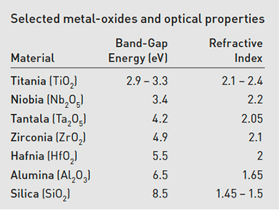
Broadly speaking, highly transparent optical-coating-layer materials, because of their negligible optical absorption, exhibit the highest LIDTs. And the best materials of this type are metal oxides, whose high transparencies derive from their large band gaps. A more nuanced picture, however, requires a quick review of the ways lasers can damage optical coatings and components.
Laser-induced damage mechanisms can be divided into extrinsic and intrinsic types. Each type couples optical energy into the molecular structure of a coating or substrate in different ways and on different timescales. This leads either to a structural change such as a melt, scald or blister, or to catastrophic structural damage. Upon subsequent exposure to laser pulses, the damage may or may not continue to grow—that is, propagate. But all damage is permanent and serves to scatter or further absorb laser light. And the density and severity of damage sites that can be tolerated before an optic in a beam train must be replaced hinges on the system’s optical performance requirements in a particular high-energy laser application.
Extrinsic damage
Extrinsic damage involves optical absorption by opaque nanoscale and microscale defects, such as particulates, contaminants or microstructural flaws, within an otherwise high-LIDT material. Such defects—ubiquitous and hard to avoid or eliminate in optical coating and processing environments—range from particulates present because of poorly enforced cleanroom and optics-handling and -cleaning protocols, to substrate surface scratches or digs, subsurface microfractures, and contamination by trace levels of polishing compounds, to microstructural imperfections within layers or at their interfaces.
Extrinsic damage occurs when absorbed optical energy at such defect sites couples through heat-transfer processes into phonon excitations and, eventually, permanent change or catastrophic damage to the material’s structure. Both the optical-absorption and heat-transfer processes occur within time durations of long (nanosecond and longer) laser pulses. Minimizing extrinsic defects is, of course, essential to optimizing an optical coating’s LIDT.
Intrinsic damage
Intrinsic damage stems from direct multiphoton coupling between intense laser electric fields and the optical coating’s electronic structure at the molecular level, leading to free electrons in the material through multiphoton ionization or excitations into electronic conduction bands. The free electrons can transfer energy into phonon excitations and heat through collisions with atoms in the material structure. Heat-transfer processes subsequently lead to bulk damage to the material.
Photon–electron interaction timescales correspond to those of electronic motion and transitions in molecules (around 10–13 s to 10–15 s), and corresponding pulse durations (sub-picosecond to femtosecond) are categorized as short-pulse in the context of laser-induced damage. But, as with extrinsic damage, the subsequent heat-transfer processes that cause bulk damage play out on nanosecond and longer time scales.
It was recognized early on that laser-induced damage begins to be a problem for an optic when its coated surface is exposed to as little as 1 J of laser energy over an area of 1 cm2.
Molecular-level electronic-structure defects that interact strongly with high-energy-laser electric fields are important to intrinsic damage. Such defects—for example, metal impurities that readily supply free electrons to conduction bands, or intraband electronic states of high-band-gap coating molecules associated with impurities or voids at the molecular level that can form during coating deposition—are ubiquitous as well. Yet intrinsic damage mechanisms also threaten defect-free areas of highly transparent thin-film materials, because the multiphoton excitations of intrinsic damage can bridge the large electronic band gaps of transparent materials.
Nonetheless, photon–electron interactions are more likely to produce free electrons at defect sites than at defect-free regions of high-transparency coatings. So minimizing intrinsic damage requires the use of ultra-high-purity coating-layer materials, especially with respect to iron and other metallic conductive impurities. Also, for metal-oxide thin-film layers, adequate oxygen enrichment in reactive-coating deposition is important for producing stoichiometrically correct layers with fewer intra-band-defect electronic states.
Multiple simultaneous mechanisms
Finally, both extrinsic and intrinsic damage mechanisms can be at work at the same time—particularly for laser pulses between the sub-picosecond short-pulse regime of intrinsic damage and the nanosecond long-pulse regime of extrinsic damage. Laser-induced damage for this intermediate pulse regime is particularly challenging to understand.
Photon energy and its dependence on wavelength also affect both extrinsic and intrinsic laser-induced damage. Starting from around 1 eV at a wavelength of 1000 nm, photon energies range up to a few eV or more at visible and UV wavelengths, and down to smaller fractions of an eV into the infrared. In general, fewer photons at higher photon energies are required for optical energy absorption in extrinsic damage as well as for multi-photon excitation and ionization in intrinsic damage. So, less laser fluence usually causes laser-induced damage at shorter wavelengths compared to longer wavelengths. (More information on damage test protocols is online at optica-opn.org/link/hel-coatings.)
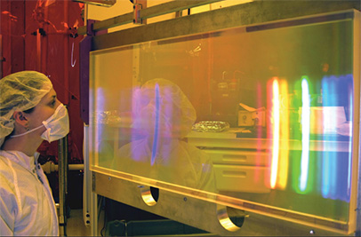 Claire Smith inspects a 91×42-cm2 MLD grating produced by PGL. The groove density is 1740 lines/mm. The MLD coating consists of HfO2/SiO2 layer pairs. [Courtesy of PGL]
Meter-class grating technology for CPA
The first efforts to apply chirped-pulse amplification (CPA) to the LLNL Nova laser used meter-class gold gratings. But gold’s low LIDT constitutes a major limitation for this application. State-of-the-art meter-class grating technology now relies on specialized reflective multilayer dielectric (MLD) grating coatings deposited onto large substrates. The grating itself is then fabricated in the outer coating layer using laser-based interference lithography patterning of the grating structure, together with photoresist coating, reactive-ion etching, and precision cleaning processes.
LLNL has developed these grating fabrication capabilities using MLD grating coatings produced on meter-class substrates by third-party vendors. Other government laboratories often cooperate with LLNL to obtain large MLD gratings. Among commercial optics manufacturers, Plymouth Grating Laboratory (PGL) has set itself apart by specializing in the fabrication technology and capability to produce these large high-LIDT MLD gratings. PGL has perfected the required laser patterning techniques using its Nanoruler technology, as well as its reactive-ion-beam etching techniques; the firm is also expert in the design and production of the MLD coatings on meter-class optics.
While these examples show that high-LIDT MLD gratings for high-energy laser CPA applications can be acquired, there are definite challenges. This is due not only to the limited number of suitable government laboratory or commercial manufacturers, but also to complications in coordinating between the production of the MLD coatings on large substrates and the fabrication of gratings onto those coatings. Even so, MLD gratings on large optics can be truly remarkable and an impressive sight to behold.
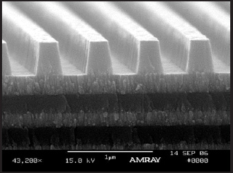
SEM image of the groove structure in the outer SiO2 layer for a PGL MLD grating. Such gratings provide a typical LIDT of 2.5 J/cm2 for 10-ps and longer pulses. [Courtesy of PGL]
Large-scale high-energy laser facilities
With the preceding discussion of damage physics as background, we can now explore how coatings research has shaped the emergence of high-energy laser facilities in recent decades.
It was recognized early on that laser-induced damage begins to be a problem for an optic when its coated surface is exposed to as little as 1 J of laser energy over an area of 1 cm2—and that a way to mitigate this damage risk lay simply in choosing appropriately sized optics. For example, a large-scale laser system using meter-class optics could handle laser pulses of nanosecond duration, amplified to pulse energies of a few kJ and delivering output powers of greater than 1 terawatt, with some, but likely low, risk of laser-induced damage to the optics.
In the United States, the Lawrence Livermore National Laboratory (LLNL), using this meter-class-optics approach, succeeded during the mid-1980s in building and operating the terawatt-scale Nova laser. The development of chirped-pulse amplification (CPA), by future Nobel laureates and Optica Fellows Gerard Mourou and Donna Strickland, opened additional avenues. By the early 1990s LLNL had implemented CPA by modifying the Nova laser with meter-class reflective gold gratings and using the grating diffraction to temporally re-compress amplified chirped pulses into very-high-energy short pulses delivering more than 1 petawatt of output power.
Since this early work, large-scale terawatt-, petawatt- and even exawatt-class laser systems have emerged worldwide—primarily at government-supported laboratories, owing to the major investments required to build, equip, staff and operate them. A few examples include the LLNL National Ignition Facility (NIF) and the Laboratory for Laser Energetics (LLE) in the United States; the Laser MegaJoule (LMJ) site in France; the Shenguang lasers in China; the Central Laser Facility and the Orion laser in England; the LFEX petawatt laser in Japan; and the Extreme Light Infrastructure (ELI) Beamlines facility in the Czech Republic.
Such facilities engage in a wide range of investigations employing high-energy-density plasmas and laser-driven acceleration of electrons and ions, with applications in fields as diverse as laboratory astrophysics, biochemistry, materials science and medical imaging and diagnostics. Most large-scale laser facilities dedicate time in their laser shot schedules for experiments by external users.
For some of these facilities, such as NIF—whose system of 192 beam trains can deliver more than 1 MJ of energy within a small focal volume—an overarching, not yet fully achieved goal is to create high-energy-density plasmas that support controlled, sustainable ICF. A significant, encouraging milestone on this quest was recently achieved at NIF with the production of so-called burning plasmas—high-energy-density plasmas that briefly sustain themselves by the heat of their own nuclear fusion reactions.
Large-scale high-energy laser systems have been enabled by high-LIDT optical coatings on meter-class substrates.
Coatings on meter-class substrates
Large-scale high-energy laser systems such as those described above have been enabled by high-LIDT optical coatings on meter-class substrates. These coatings range from high-reflection (HR) mirror coatings, to antireflection (AR) coatings for windows and lenses, to polarizer and dichroic beam splitter coatings. To meet the demand from such facilities over the past 30 years, coating manufacturers have significantly expanded their operations with large vacuum chambers and upgraded capacity to provide coatings for meter-class optics in production quantities ranging from the hundreds to the thousands for some multi-beam laser systems.
Continuing large-optics coating operations after the end of major production contracts tied to individual facilities is often not viable. A few companies, however, such as Okamoto Optics in Japan and Safran Reosc in France, produce coatings on just one or a few large optics at a time, whenever they are needed to replace damaged optics in a beam train. Nevertheless, the demand by large-scale laser facilities for coatings on large optics at any given time often exceeds the production capacity of available meter-class-optical-coating companies.
Most large government laser facilities have established in-house coating operations for at least some critical large optics. This is particularly true for sol-gel coating of debris-shield windows using silicate-based liquids. The porous SiO2 structure of sol-gel coatings provides good AR and LIDT properties, but requires delicate handling because of its fragility. Both LLNL and LMJ, for example, have extensive in-house sol-gel coating capabilities (see opening photo). In China, the Shanghai Institute of Optics and Fine Mechanics (SIOM) provides high-LIDT coating research and support for Chinese large-scale laser facilities and can produce coatings for large optics. LLE established in-house large-optics coating capabilities in the early 1980s, and its coating operation has become an international research leader in this area.
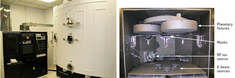 Exterior (left) and interior (right) views of the 2.3×2.3×1.8-m large-optics vacuum coating chamber at Sandia National Laboratories. The chamber, in a Class 100 cleanroom, is equipped for electron-beam evaporation of coating materials, with or without ion-assisted deposition provided by an RF ion source. The planetary rotational fixtures can accommodate optical substrates of dimension up to 1.2 m, with masking to provide for thickness uniformity of coating layers on large substrates. [Courtesy of Sandia National Laboratories]
Sandia National Laboratories (SNL) also established an in-house coating facility with a large vacuum coating chamber for meter-class optics, dedicated to producing coatings for the high energy Z-Backlighter lasers that provide diagnostics for SNL’s pulsed-power radiation source, the Z-Machine. The coated meter-class optics that emerge from such efforts can be very beautiful and even awe-inspiring; an example is the Z-Backlighter mirror shown on p. 30.
Other government laboratories have established or are establishing in-house large-optics coating capabilities, and major government research organizations have also pushed the state of the art in large-optics coatings by supporting research efforts at universities and within the private sector. The result of this effort is a strong, cooperative world-wide community centered around large-scale high-energy-laser coating technology.
Recent high-LIDT coating research
Contemporary state-of-the-art development of high-LIDT coatings relies on sophisticated optical thin-film design and analysis software such as OptiLayer and Essential Macleod to evaluate optical electric-field standing-wave intensities within coating layers. This provides ways to explore the tradeoffs between the coating’s optical and LIDT performance targets. Coating designs with low electric-field intensities within low-band-gap layers and high intensities within high-band-gap layers favor higher LIDTs.
Recent research led by Ella Field of SNL employed such electric-field analyses, using OptiLayer, to evaluate a dichroic coating for the Z-Backlighter lasers. The coating design is based on HfO2/SiO2 layer pairs to provide high transmission at 527 nm and high reflection at 1054 nm for an incidence angle of 22.5o. The electric-field patterns showed peak intensities at both laser-induced-damage test wavelengths, 532 nm and 1064 nm, in the outer two HfO2 and SiO2 layers; further, high intensities at 532 nm persist within the inner SiO2 layers and at some inner layer interfaces.
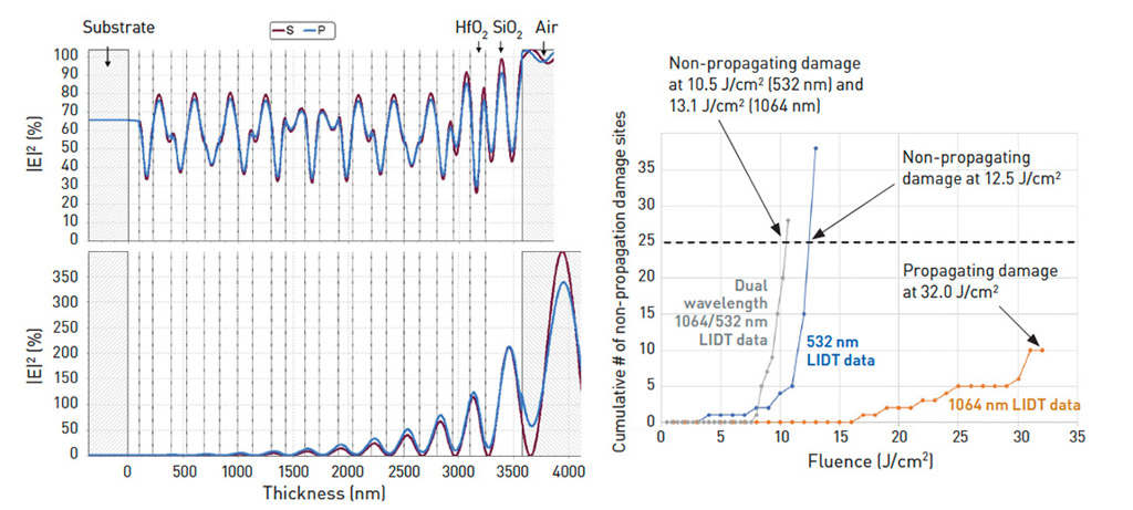 Electric-field standing-wave intensity models (S and P polarizations) at 532 nm (top left) and 1064 nm (bottom left) for a HfO2/SiO2 dichroic coating design, assuming an incidence angle of 22.5°. Vertical lines show layer interfaces. Right: Results of laser-damage tests in the ns-pulse regime on the designed coating as deposited highlight LIDTs that are higher for 1064-nm compared with 532-nm laser radiation, and still lower for 1064/532-nm dual-wavelength laser radiation. [Enlarge image] [E.S. Field et al., Proc. SPIE 11173, 1117314 (2019); reprinted with permission]
This suggested that the coating’s 532-nm LIDT would be lower than the 1064-nm LIDT not only because of the higher 532-nm photon energy, but because the 532-nm electric-field intensity peaks are present not just in the outer layers but throughout the coating. Laser-induced damage tests performed by Spica Technologies Inc. confirmed the predictions of the electric-field models—and also revealed, in dual 1064-nm/532-nm tests, that the damage caused by the higher-energy 532-nm photons is enhanced by the presence of the lower-energy 1064 nm photons. These results represent what can be expected for the meter-class dichroic beam splitter in the actual dual-wavelength Z-Backlighter laser beam train.
Another important aspect of high-LIDT coating design is the reverse relationship between the band gaps and refractive indices of the metal-oxide-layer materials. SiO2, with the highest band-gap energy (and, accordingly, the highest resistance to laser-induced damage) and the lowest refractive index, is the preferred low-index-layer material for high LIDT coatings. For the high-index metal oxide layers that will be paired with the SiO2 layers, careful trade-offs are required between the best high/low index contrast ratios for efficient optical performance and the band-gap energies for superior LIDT performance.
A 2020 mirror-coating study led by Meiping Zhu of SIOM took an innovative approach to these issues, proposing a new class of so-called nanolaminate coating layers that can optimize the band-gap/refractive-index tradeoffs more effectively than the traditional approach. The study focused on a mirror coating reflecting 355-nm UV laser light at 45o angle of incidence. In this case, the mirror coating standing-wave electric fields are like those for 1064 nm in the SNL study, exhibiting intensity peaks that are very strong in the outer layers and diminish to be very weak in the inner layers.
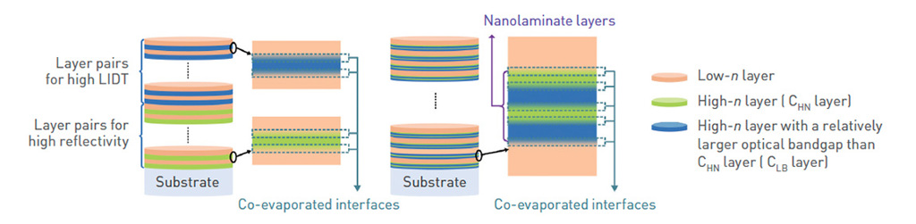 Mirror coatings with layer interfaces co-evaporated from adjacent layer materials. In traditional approaches (left), low-index (Low-n) layers alternate with high-index layers (inner CHN layers and outer, larger-band-gap CLB layers). In nanolaminate approaches (right), low-index layers alternate throughout the coating with nanolaminate high-index layers comprised of alternating CHN and CLB nanolayers, providing improved optical performance and laser-damage resistance over traditional approaches. [Enlarge image] [M. Zhu et al., Light Sci. Appl. 9, 20 (2020); CC-BY 4.0]
In traditional approaches to such a coating, the larger-band-gap CLB material provides resistance to laser-induced damage in the outer layers, where the electric fields are most intense, while the higher-index CHN material, which is more vulnerable to laser-induced damage, provides its optical-performance benefit in the inner layers, where the electric-field intensities are very weak.
The science and production of coatings for high-energy lasers will continue to advance as a rich, dynamic part of optical technology.
In the nanolaminate approach developed by Zhu and colleagues, high-index nanolaminate layers, comprising alternating high-index CHN and CLB nanolayers, in turn alternate with the low-index layers throughout the entire coating. This multilayer arrangement provides an optimal combination of high-index and high-LIDT properties of the CHN and CLB materials. For the specific UV mirror coating in the study, the layer materials were SiO2 (Low-n), HfO2 (CHN) and Al2O3 (CLB). Overall, the study found that the nanolaminate coating layers distributed throughout such a multilayer stack provide a blend of high-index Al2O3 and HfO2 layers that is superior to that of the traditional approach in terms of reflectivity and LIDT performance.
Research such as the examples outlined above shows that high-LIDT optical-coating technology—a key factor that has enabled high-energy-laser science and the quest to produce high-energy-density plasmas—remains an area of active development. The recent attainment of the burning-plasma milestone toward sustained ICF, achieved at LLNL’s high-energy NIF laser system, is just the latest breakthrough to highlight the enabling role of these ongoing coating efforts. The science and production of coatings for high-energy lasers will continue to advance as a rich, dynamic part of optical technology.
John Bellum is a consultant in optical coatings with Coherent Technologies, Albuquerque, NM, USA, and a distributor for OptiLayer Thin Film Software.
References and Resources
-
J. Bellum et al. “Production of optical coatings resistant to damage by petawatt-class laser pulses,” in K. Jakubczak (ed.), Lasers—Applications in Science and Industry (InTechOpen, Rijeka, Croatia, 2011).
-
P. Rambo et al. “Sandia’s Z-Backlighter laser facility,” Proc. SPIE 10014, 100140Z (2016).
-
C.J. Stolz and R.A. Negres. “Ten-year summary of the Boulder Damage Symposium annual thin-film laser damage competition,” Opt. Eng. 57, 121910 (2018).
-
C. Danson et al. “Petawatt and exawatt class lasers worldwide,” High Power Laser Sci. Eng. 7, e54 (2019).
-
E.S. Field et al. “Dual-wavelength laser-induced damage threshold of a HfO2/SiO2 dichroic coating developed for high transmission at 527 nm and high reflection at 1054 nm,” Proc. SPIE 11173, 1117314 (2019).
-
J.B. Oliver et al. “Large-aperture coatings for fusion-class laser systems,” Appl. Opt. 59, A7 (2020).
-
M. Zhu. et al. “Nanolaminate-based design for UV laser mirror coatings,” Light Sci. Appl. 9, 20 (2020).
-
L. Lamaignere et al. “Round-robin measurements of the laser-induced damage threshold with sub-picosecond pulses on optical single layers,” Opt. Eng. 60, 031005 (2021).
-
A.B. Zylstra et al. “Burning plasma achieved in inertial fusion,” Nature 601, 542 (2022).
For additional resources, visit: optica-opn.org/link/hel-coatings.