
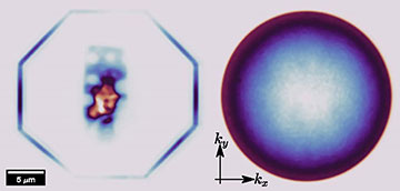
Using hBN as a waveguide enabled the light emission (left) and the angle of the emitted light (right) to be measured for a 2D heterostructure [Image: US Naval Research Laboratory/Nicholas Proscia]
Researchers in the United States have shown that hexagonal boron nitride (hBN), a layered insulator with a similar structure to graphite, can provide an effective optical waveguide for heterostructures containing light-emitting 2D materials (Adv. Mat., doi: 10.1002/adma.202309777). While hBN has already become critically important as an encapsulating layer that preserves and enhances the optoelectronic properties of these 2D structures, the researchers found that hBN slabs can also couple the light emission from the atomically thin layer into fundamental waveguide modes.
"We knew that hexagonal boron nitride would lead to outstanding optical properties in our samples, but none of us expected that it would also act as a waveguide," said Samuel Lagasse from the US Naval Research Laboratory (NRL). "Since hBN is used so widely in 2D material–based devices, this novel usage as an optical waveguide potentially has wide-ranging impacts."
2D semiconductors
The NRL-led study focused on a pair of 2D semiconductors, molybdenum selenide and tungsten selenide, that emit light in the visible and near-infrared. Materials of this type are appealing for future optoelectronic devices, but probing their optical properties has proved difficult because their in-plane light emission cannot easily be detected with a standard microscope configuration. Various experimental schemes have been tried, but they can perturb the characteristics of the 2D materials and add extra complexity to the fabrication process.
By tuning the thickness of the hBN slabs, they showed that the light emission can be coupled into waveguide modes without compromising the intrinsic properties of the 2D material.
In this case, however, the researchers stacked single layers of the light-emitting material within two hBN slabs, etching the heterostructure into an octagonal shape to enable easy optical access. By tuning the thickness of the hBN slabs, they showed that the light emission can be coupled into waveguide modes without compromising the intrinsic properties of the 2D material. A spectrometer at the edge of the structures collected the guided light, revealing the expected emission characteristics for each of the two materials.
Expanding the toolkit
Numerical simulations created by the team also offer a toolkit for designing other 2D structures that exploit these hBN waveguides. They show that single-mode operation over a wide range of relevant wavelengths can be achieved with a total hBN thickness of 200 to 250 nm, with shorter wavelengths benefitting from thicker slabs. Meanwhile, hBN layers thinner than about 50 nm do not act as an optical waveguide.
The numerical results also indicate that most of the light is guided in the first few fundamental modes, with less than 10 percent reaching higher-order or hybrid modes. The properties of the guided light can also be altered by changing the position of the light emitter within the heterostructure, a finding that could inform the design of future optoelectronic devices.
