
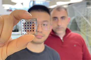
Yongjie Wang shows off the highly absorbing, disorder-engineered device made by him and his colleagues at ICFO in Barcelona, Spain. Group leader Gerasimos Konstantatos is seen in the background. [Image: ©ICFO]
Ideally, a solar cell would be efficient, light, cheap and environmentally friendly. That combination has, to date, proved elusive. But scientists in Spain and the United Kingdom reckon they might have the answer: ultrathin devices made from nanocrystals of silver bismuth sulphide (AgBiS2).
The researchers have shown that, by engineering the distribution of positively charged ions within such nanocrystals, they can boost the absorption of incoming light to unprecedented levels and, in doing so, convert about 9% of the solar energy to electricity (Nat. Photon., doi: 10.1038/s41566-021-00950-4). That is still only about a third of the best silicon cells, but they are confident they can boost this figure to around 15%—thereby making the technology commercially attractive as a low-cost, versatile alternative to standard photovoltaics.
Tackling the light-absorbing material
Ultrathin solar cells offer the prospect of fairly straightforward manufacturing techniques with less material consumption, and the possibility of flexible, lightweight devices that can be incorporated into buildings or even clothing. However, their very thinness makes them less able to absorb photons and thereby limits the photocurrents they can generate.
Improving the performance of such cells is usually done by adding structures to them, such as photonic cavities or plasmonic gratings, which trap and focus light on to their surfaces. But these structures make the devices more complex and expensive to produce.
In the latest work, Gerasimos Konstantatos and colleagues at ICFO in Barcelona, Spain, instead modify the properties of the light-absorbing material itself. Their material consists of nanometer-scale crystals of colloidal AgBiS2, which is a non-toxic semiconductor formed from naturally abundant elements.
Six years ago, the researchers showed that solution processing could be used to fashion the nanocrystals into an active photovoltaic layer just 35 nm thick that yielded a power conversion efficiency of 6.3%.
Bringing order to disorder
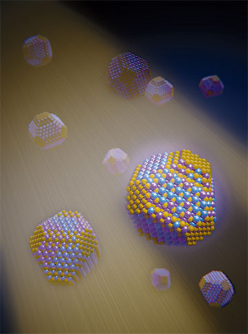
Illustration of the homogenous cation distribution achieved inside the AgBiS2 nanocrystals. [Image: ©ICFO / Scixel]
Now, as they report in Nature Photonics, the researchers have shown how to boost that efficiency by engineering the disorder of cations within the nanocrystals to enhance the material’s absorption coefficient. The dynamics of crystal growth naturally lead to an uneven distribution of the material’s constituent atoms, with regions containing an excess of either silver or bismuth. This, in turn, leads to a patchiness in the semiconductor’s electron cloud and a consequent impairment of photon absorption.
Working with scientists at University College London and Imperial College London in the UK, the researchers used computer simulation to work out how a homogenization of the atomic distribution would boost the absorption coefficient. They also calculated how much energy would be needed to induce the necessary migration of ions.
Establishing the latter to be a mere 17.4 meV per atom, they carried out low-temperature annealing on the AgBiS2 and measured the consequent change in absorption. They did so at temperatures of 80°C, 115°C and 150°C, while varying the incoming wavelength between about 400 nm and 1400 nm. They found they could enhance the absorption coefficient by as much as a factor of two compared to the non-annealed state, making it, they say, 5 to 10 times more absorbing than that of any material currently used to make photovoltaic cells.
New and improved ultrathin solar cell
Having measured such impressive optical absorption, the researchers went on to produce a new and improved ultrathin solar cell. Built on a substrate of glass and indium tin oxide, the cell featured a 30 nm-thick layer of AgBiS2 and a 4 nm-thick layer of poly(triaryl amine) to block electrons. With this combination, they achieved power conversion efficiencies as high as 9.2%. These results were corroborated by an independent lab in Newport, USA, which certified an efficiency of 8.9% under full-sun illumination.
Konstantatos and colleagues point out that some incoming light is still lost through reflection off the cell’s surface, implying that the addition of an antireflection layer should further improve the device’s performance—pushing up the efficiency, they estimate, to around 11%.
They add that the cell is also quite stable, retaining its performance after four months on a shelf in ambient conditions and seeing its efficiency drop by just 15% after being exposed for 10 hours to solar radiation yielding maximum power—even though unprotected by encapsulation. Plus, they say, the cell should also be quite cheap to make. Allowing for the significant expense of encapsulation, they work out that a slashing of cell thickness from the standard 500 nm to 30 nm would nearly halve the overall cost of a cell.
Writing a commentary piece in Nature Photonics to accompany the research, Xiaoyu Yang and Rui Zhu of Peking University in China describe the work as a “milestone” in the development of ultrathin solar cells. But they caution that further raising the efficiency will not be easy. Weak absorption of low-energy photons could prove an impediment to generating greater photocurrents, they argue, while nonradiative recombination losses impair the photovoltage. The synthesis of high-quality crystals with fewer structural defects, cleaner surfaces and less ion migration should help to reduce such losses, they say.