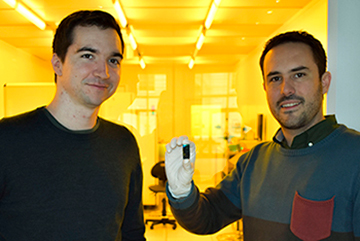
Lead authors Blair Morrison (left) and Alvaro Casas-Bedoya (right) with one of the CUDOS team’s integrated silicon-As2S3 chips. [Image: AINST]
Australian researchers have developed methods to integrate high-Brillouin-gain chalcogenide glasses on silicon, and have fashioned compact, chip-scale devices using those techniques—including, according to the team, “the first demonstration, to our knowledge, of Brillouin lasing in a planar integrated circuit” (Optica, doi: 10.1364/OPTICA.4.000847). The researchers believe that the work could help leverage stimulated Brillouin scattering (SBS), which they characterize as “one of the strongest nonlinearities known to optics,” in fully integrated devices such as integrated optoelectronic oscillators, microwave photonic filters and compact optical gyroscopes.
Beating nonlinear losses
SBS involves the interaction of high-intensity light with matter; light creates acoustic vibrations that in turn scatter the light. While the phenomenon can create problems for long-haul fiber communications, it also opens opportunities for applications, as it offers the possibility of strong nonlinear gains, particularly for microwave applications (see “Harnessing On-Chip SBS,” OPN, February 2015). Getting these devices effectively into a CMOS-compatible platform, however, has proved something of a puzzle, as SBS devices in silicon have suffered from nonlinear-loss behavior at telecom wavelengths.
To get around those issues, a team led by OSA Fellow Ben Eggleton of the University of Sydney’s Center for Ultrahigh-bandwidth Devices for Optical Systems (CUDOS) has been exploring the potential of a hybrid approach integrating silicon with chalcogenide glasses. These glasses—which combine chalcogenide elements such as sulfur or selenium with network-forming elements such as arsenic or phosphorus—offer very high Brillouin gains and avoid the loss behavior of silicon at the wavelengths relevant for optical communications. Finding a way to integrate chalcogenide optical circuits onto silicon would, the CUDOS team reasoned, offer a way to make those circuits mass-manufacturable, given silicon’s role as an industry-standard platform for photonic integration.
Putting As2S3 on silicon
To get at that integrated system, the CUDOS researchers, including lead authors (and OSA members) Blair Morrison and Alvaro Casas-Bedoya, began with a silicon wafer created at the imec research foundry in Belgium. Then, the team took the wafer back to the Australian National University’s Laser Physics Center, and there thermally deposited a layer of amorphous arsenic trisulfide (As2S3) into a 0.1-mm-by-4-mm open silicon region on the wafer. Electron beam lithography and inductively coupled plasma etching shaped the As2S3 glass layer into nanowire waveguides, the active SBS section of the chip; a linearly tapered silicon waveguide linked that active section to the chip’s base silicon section.
Using the technique, the team fabricated several devices, including an on-chip hybrid circuit including an As2S3 spiral waveguide and a chip with a tiny planar As2S3 ring resonator. In a series of pump-probe experiments, the researchers found that the spiral-waveguide device achieved “an order-of-magnitude increase in Brillouin amplification.” And by tuning a pump light source precisely to the Brillouin shift of the As2S3 glass in the ring resonator, the group was create a Brillouin laser on the chip.
Scalable method
Putting a chalcogenide glass together with CMOS fabrication, lead author Casas-Bedoya noted in a press release, allowed the team to maintain “the key advantages of both the silicon and the glass,” and to create “a functional and efficient ultra-compact optical circuit.” CUDOS director Eggleton added that the creation of a platform that is “more compatible” with existing CMOS processes offers the prospect of scalable integration of “active and passive components, such as detectors and modulators, required for advanced applications.”
The authors on the study included researchers from CUDOS and the Australian Institute for Nanoscale Science and Technology (AINST) at the University of Sydney, from Australian National University in Canberra, and RMIT University in Melbourne.
