
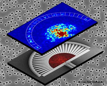
Top: near-IR optical image of the random spectrometer, probe signal at λ = 1500 nm. White boxes mark the position of detection channels at the end of each waveguide. Bottom: TE-polarized light diffuses through a semicircular silicon structure with randomly patterned holes that scatters the light and sends it down the waveguides to the detector channels.
Researchers at Yale University have demonstrated the first microspectrometer with subnanometer resolution based on a disordered photonic chip (Nat. Phot. 7, 746), enabling high resolution in a micron-scale footprint. Typically, light scattering is a challenge to overcome in an optical system. But in the past decade, research has focused on using scattering to fold the optical paths in spectroscopy, so that the resolution of the system is no longer limited by the physical dimensions of the device.
Professor of applied physics and OSA Fellow Hui Cao and her team built an on-chip semi-circular scattering structure the width of a human hair to take advantage of multiple scattering. The structure has at its center a semicircular plane of silicon patterned with randomly positioned air holes surrounded by a reflecting layer of photonic crystal that confines light inside the scattering structure. Scattered light diffuses through the semicircular patterned plane into 25 tapered defect waveguide channels tangent to the circumference, and into detectors at the end of each waveguide.
“The use of multiple scattering of light in the random structure enhances the spectral resolution and reduces the foot print, which enables tiny, portable spectrometers with high resolution and a broad range of applications,” says Cao.
Using polarized laser light of λ = 1500 nm, the team achieved a spectral resolution of 0.75 nm in a 25-µm-radius structure, approaching the resolution of tabletop-sized spectrometers. The diminutive spectrometer has potential for volume fabrication, which means it can be manufactured cheaply, and has potential in diverse outside-the-lab applications like fuel transport, textiles, and optical systems.